- 您现在的位置:买卖IC网 > PDF目录361766 > W15NK90Z (意法半导体) N-CHANNEL 900V-0.40ohm-15A TO-247 Zener-Protected SuperMESH MOSFET PDF资料下载
参数资料
| 型号: | W15NK90Z |
| 厂商: | 意法半导体 |
| 英文描述: | N-CHANNEL 900V-0.40ohm-15A TO-247 Zener-Protected SuperMESH MOSFET |
| 中文描述: | N沟道900V - 0.40ohm - 15A条,247齐纳MOSFET的保护SuperMESH |
| 文件页数: | 3/9页 |
| 文件大小: | 220K |
| 代理商: | W15NK90Z |
3/9
STW15NK90Z
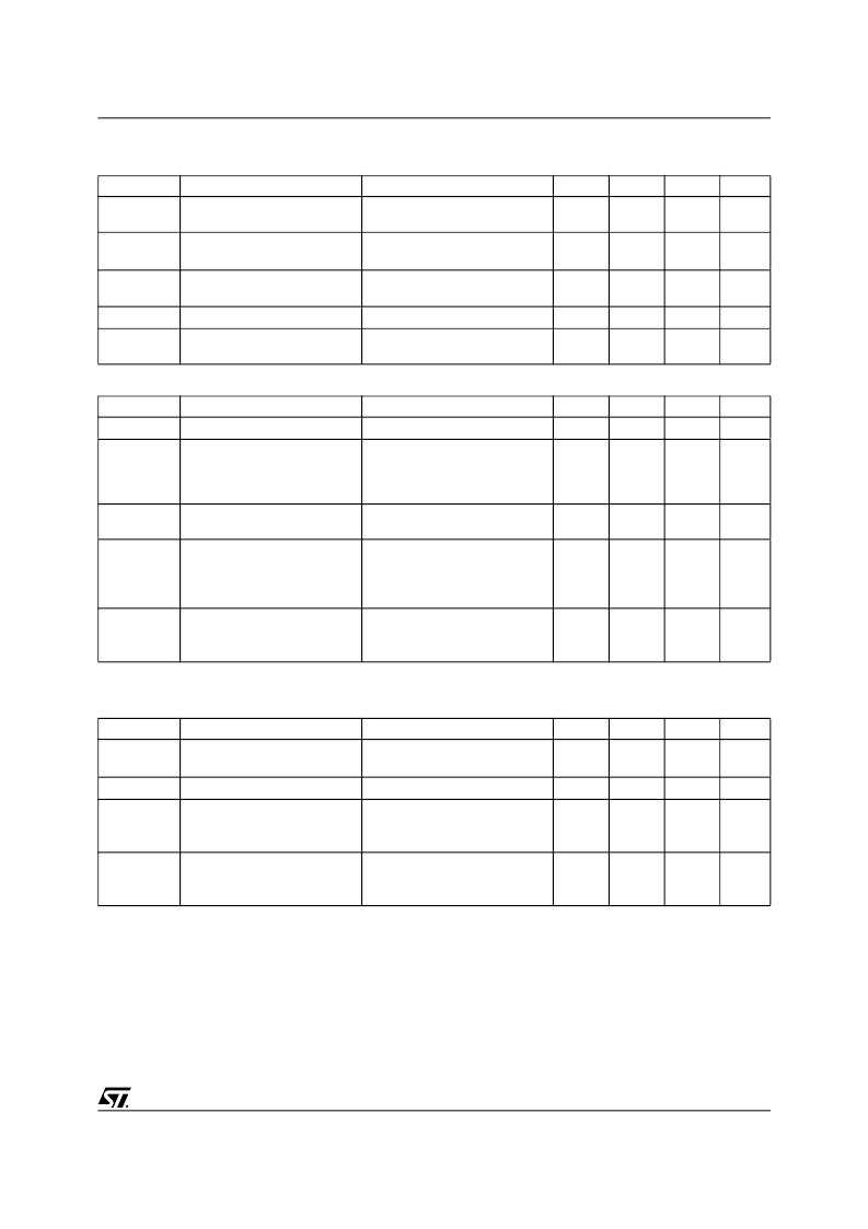
ELECTRICAL CHARACTERISTICS
(T
CASE
=25
°
C UNLESS OTHERWISE SPECIFIED)
ON/OFF
Symbol
Parameter
V
(BR)DSS
Drain-source
Breakdown Voltage
I
DSS
Zero Gate Voltage
Drain Current (V
GS
= 0)
V
DS
= Max Rating, T
C
= 125
°
C
I
GSS
Gate-body Leakage
Current (V
DS
= 0)
V
GS(th)
Gate Threshold Voltage
V
DS
= V
GS
, I
D
= 150 μA
R
DS(on)
Static Drain-source On
Resistance
DYNAMIC
Symbol
g
fs
(1)
C
iss
C
oss
C
rss
SOURCE DRAIN DIODE
Symbol
I
SD
I
SDM
(2)
V
SD
(1)
t
rr
Q
rr
I
RRM
t
rr
Q
rr
I
RRM
Note: 1. Pulsed: Pulse duration = 300 μs, duty cycle 1.5 %.
2. Pulse width limited by safe operating area.
3. C
oss eq.
is defined as a constant equivalent capacitance giving the same charging time as C
oss
when V
DS
increases from 0 to 80%
V
DSS
.
Test Conditions
I
D
= 1 mA, V
GS
= 0
Min.
900
Typ.
Max.
Unit
V
V
DS
= Max Rating
1
50
μA
μA
V
GS
= ± 20V
±10
μA
3
3.75
4.5
V
V
GS
= 10V, I
D
= 7.5 A
0.40
0.55
Parameter
Test Conditions
V
DS
= 15 V
,
I
D
= 7.5 A
V
DS
= 25V, f = 1 MHz, V
GS
= 0
Min.
Typ.
15
Max.
Unit
S
Forward Transconductance
Input Capacitance
Output Capacitance
Reverse Transfer
Capacitance
Equivalent Output
Capacitance
Turn-on Delay Time
Rise Time
Turn-off Delay Time
Fall Time
6100
465
96
pF
pF
pF
C
oss eq.
(3)
V
GS
= 0V, V
DS
= 0V to 720V
230
pF
t
d(on)
t
r
t
d(off)
t
f
Q
g
Q
gs
Q
gd
V
DD
= 450 V, I
D
= 7.5 A
R
G
= 4.7
V
GS
= 10 V
(Resistive Load see, Figure 3)
42
27
135
35
ns
ns
ns
ns
Total Gate Charge
Gate-Source Charge
Gate-Drain Charge
V
DD
= 720 V, I
D
= 15 A,
V
GS
= 10V
190
56
70
256
nC
nC
nC
Parameter
Test Conditions
Min.
Typ.
Max.
15
60
Unit
A
A
Source-drain Current
Source-drain Current (pulsed)
Forward On Voltage
I
SD
= 15 A, V
GS
= 0
I
SD
= 15 A, di/dt = 100 A/μs
V
DD
= 100 V, T
j
= 25
°
C
(see test circuit, Figure 5)
1.6
V
Reverse Recovery Time
Reverse Recovery Charge
Reverse Recovery Current
748
10.5
28
ns
μC
A
Reverse Recovery Time
Reverse Recovery Charge
Reverse Recovery Current
I
SD
= 15 A, di/dt = 100 A/μs
V
DD
= 100 V, T
j
= 150
°
C
(see test circuit, Figure 5)
900
13
28.5
ns
μC
A
相关PDF资料 |
PDF描述 |
|---|---|
| W162-09G | NINE DISTRIBUTED-OUTPUT CLOCK DRIVER|CMOS|SOP|16PIN|PLASTIC |
| W162-19G | NINE DISTRIBUTED-OUTPUT CLOCK DRIVER|CMOS|SOP|16PIN|PLASTIC |
| W163-05G | Five Distributed-Output Clock Driver |
| W163-15G | FIVE DISTRIBUTED-OUTPUT CLOCK DRIVER|CMOS|SOP|8PIN|PLASTIC |
| W164G | Industrial Control IC |
相关代理商/技术参数 |
参数描述 |
|---|---|
| W160 | 制造商:GARRYSON 功能描述:MOUNTED POINT |
| W160A | 制造商:NSC 制造商全称:National Semiconductor 功能描述:160 Lead Cerquad, EIAJ |
| W160E12 | 制造商:OMRON INDUSTRIAL AUTOMATION 功能描述:NETWORK SERVICE UNIT (NSB) DX CODE ZA |
| W161 | 制造商:CYPRESS 制造商全称:Cypress Semiconductor 功能描述:133-MHz Spread Spectrum FTG for Pentium II Platforms |
| W16112 | 制造商:FLORIDA MISC. 功能描述: |
发布紧急采购,3分钟左右您将得到回复。