- 您现在的位置:买卖IC网 > PDF目录361766 > W162-09G NINE DISTRIBUTED-OUTPUT CLOCK DRIVER|CMOS|SOP|16PIN|PLASTIC PDF资料下载
参数资料
| 型号: | W162-09G |
| 英文描述: | NINE DISTRIBUTED-OUTPUT CLOCK DRIVER|CMOS|SOP|16PIN|PLASTIC |
| 中文描述: | 第九分布式输出时钟驱动器|的CMOS |专科| 16PIN |塑料 |
| 文件页数: | 2/7页 |
| 文件大小: | 131K |
| 代理商: | W162-09G |
W162
Document #: 38-07150 Rev. **
Page 2 of 7
Overview
The W162 products are nine-output zero delay buffers. A
Phase-Locked Loop (PLL) is used to take a time-varying signal
and provide eight copies of that same signal out.
Internal feedback is used to maximize the number of output
signals provided in the 16-pin package.
Spread Aware
Many systems being designed now utilize a technology called
Spread Spectrum Frequency Timing Generation. Cypress has
been one of the pioneers of SSFTG development, and we de-
signed this product so as not to filter off the Spread Spectrum
feature of the Reference input, assuming it exists. When a zero
delay buffer is not designed to pass the SS feature through,
the result is a significant amount of tracking skew which may
cause problems in systems requiring synchronization.
For more details on Spread Spectrum timing technology,
please see the Cypress Application note titled,
“
EMI Suppres-
sion Techniques with Spread Spectrum Frequency Timing
Generator (SSFTG) ICs.
”
Functional Description
Logic inputs provide the user the ability to turn off one or both
banks of clocks when not in use, as described in
Table 1
. Dis-
abling a bank of unused outputs will reduce jitter and power
consumption, and will also reduce the amount of EMI generat-
ed by the W162.
These same inputs allow the user to bypass the PLL entirely if
so desired. When this is done, the device no longer acts as a
zero delay buffer, it simply reverts to a standard nine-output
clock driver.
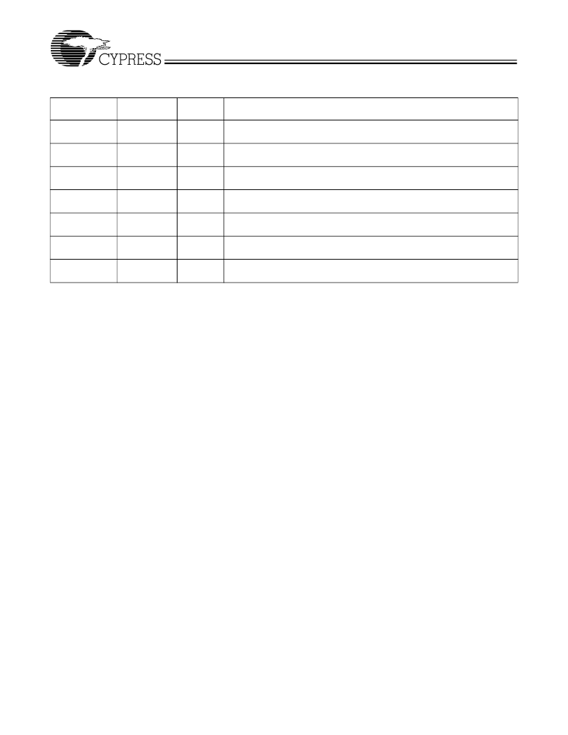
Pin Definitions
Pin Name
REF
Pin No.
1
Pin
Type
I
Pin Description
Reference Input:
The output signals QA0:3 through QB0:3 will be synchro-
nized to this signal unless the device is programmed to bypass the PLL.
Feedback Output:
This signal is used as the feedback internally to establish
the propagation delay of nearly 0.
Outputs from Bank A:
The frequency of the signals provided by these pins
is equal to the signal connected to REF.
Outputs from Bank B:
The frequency of the signals provided by these pins
is equal to the signal connected to REF.
Power Connections:
Connect to 3.3V. Use ferrite beads to help reduce noise
for optimal jitter performance.
Ground Connections:
Connect all grounds to the common system ground
plane.
Function Select Inputs:
Tie to V
DD
(HIGH, 1) or GND (LOW, 0) as desired
per
Table 1
.
QFB
16
O
QA0:3
2, 3, 14, 15
O
QB0:3
6, 7, 10, 11
O
VDD
4, 13
P
GND
5, 12
P
SEL0:1
9, 8
I
相关PDF资料 |
PDF描述 |
|---|---|
| W162-19G | NINE DISTRIBUTED-OUTPUT CLOCK DRIVER|CMOS|SOP|16PIN|PLASTIC |
| W163-05G | Five Distributed-Output Clock Driver |
| W163-15G | FIVE DISTRIBUTED-OUTPUT CLOCK DRIVER|CMOS|SOP|8PIN|PLASTIC |
| W164G | Industrial Control IC |
| W166G | Development Tools InSystem Programming ProASICPLUS Devices |
相关代理商/技术参数 |
参数描述 |
|---|---|
| W162-09GT | 制造商:Rochester Electronics LLC 功能描述:- Tape and Reel |
| W162-19G | 制造商:Cypress Semiconductor 功能描述:Zero Delay PLL Clock Driver Single 15MHz to 133MHz 16-Pin SOIC |
| W162CLR-25 | 制造商:NTE Electronics 功能描述:WIRE-SPKR 16/2 CLEAR STRANDED 25' |
| W162E11 | 制造商:OMRON INDUSTRIAL AUTOMATION 功能描述:FIT Interface to LAN DX CODE ZA |
| W162-HEA-100 | 制造商:NTE Electronics 功能描述: |
发布紧急采购,3分钟左右您将得到回复。