- 您现在的位置:买卖IC网 > PDF目录361766 > W170-01G Miscellaneous Clock Generator PDF资料下载
参数资料
| 型号: | W170-01G |
| 英文描述: | Miscellaneous Clock Generator |
| 中文描述: | 杂项时钟发生器 |
| 文件页数: | 5/6页 |
| 文件大小: | 152K |
| 代理商: | W170-01G |
W170-01
5
Document #: 38-00795-*A
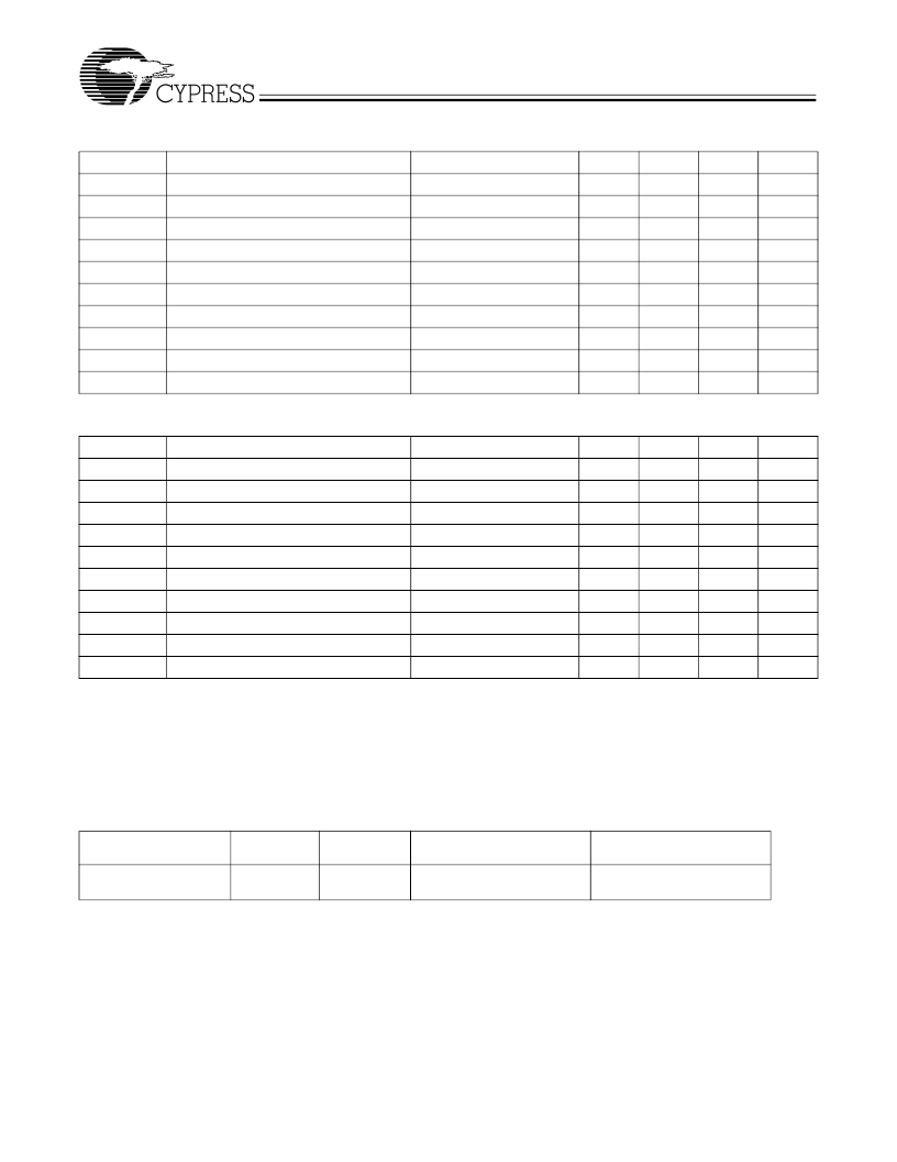
AC Electrical Characteristics:
T
A
= 0°C to +70°C or –40° to 85°C, V
DD
= 3.3V±5%
Parameter
Description
f
IN
f
OUT
Output Frequency
t
R
Output Rise Time
t
F
Output Fall Time
t
ICLKR
t
ICLKF
t
PD
t
D
Duty Cycle
t
LOCK
PLL Lock Time
t
JC
Jitter, Cycle-to-Cycle
Test Condition
OUT2 = REF
OUT1
0.8V to 2.0V, 15-pF load
2.0V to 0.8V, 15-pF load
Min.
Typ.
Max.
Unit
MHz
MHz
ns
ns
ns
ns
ps
%
ms
ps
Input Frequency
[1]
20
133
3.5
2.5
10
10
300
60
1.0
250
Input Clock Rise Time
[2]
Input Clock Fall Time
[2]
FBIN to IN (Reference Input) Skew
[3, 4]
Note 4
Note 5
Power supply stable
Note 6
40
50
AC Electrical Characteristics:
T
A
= 0°C to +70°C or –40° to 85°C, V
DD
= 5V±10%
Parameter
Description
f
IN
f
OUT
Output Frequency
t
R
Output Rise Time
t
F
Output Fall Time
t
ICLKR
t
ICLKF
t
PD
t
D
Duty Cycle
t
LOCK
PLL Lock Time
t
JC
Jitter, Cycle-to-Cycle
Notes:
1.
Input frequency is limited by output frequency range and input to output frequency multiplication factor (which is determined by circuit configuration).
2.
Longer input rise and fall time will degrade skew and jitter performance.
3.
All AC specifications are measured with a 50
transmission line, load terminated with 50
to 1.4V.
4.
Skew is measured at 1.4V on rising edges.
5.
Duty cycle is measured at 1.4V.
6.
Jitter is measured on 133-MHz signal at 1.4V, low frequency jitter = 350 ps.
7.
Duty cycle is measured at 1.4V, 120 MHz.
8.
Duty cycle at 133 MHz is 35/65 worst case.
Test Condition
OUT2 = REF
OUT1
0.8V to 2.0V, 15-pF load
2.0V to 0.8V, 15-pF load
Min.
Typ.
Max.
Unit
MHz
MHz
ns
ns
ns
ns
ps
%
ms
ps
Input Frequency
[1]
20
133
3.5
2.5
10
10
300
60
1.0
200
Input Clock Rise Time
[2]
Input Clock Fall Time
[2]
FBIN to IN (Reference Input) Skew
[3, 4]
Note 4
Note 7, 8
Power supply stable
Note 6
40
50
Ordering Information
Ordering Code
W170
Option
-01
Package
Name
Package Type
8-pin SOIC (150 mil)
Temperature Grade
Commerical (0
o
to 70
o
C)
I = Industrail (–40
o
to 85
o
C)
G
相关PDF资料 |
PDF描述 |
|---|---|
| W180-01G | Miscellaneous Clock Generator |
| W180-02G | MISCELLANEOUS CLOCK GENERATOR|CMOS|SOP|8PIN|PLASTIC |
| W180-03G | MISCELLANEOUS CLOCK GENERATOR|CMOS|SOP|8PIN|PLASTIC |
| W180-51G | MISCELLANEOUS CLOCK GENERATOR|CMOS|SOP|8PIN|PLASTIC |
| W180-52G | MISCELLANEOUS CLOCK GENERATOR|CMOS|SOP|8PIN|PLASTIC |
相关代理商/技术参数 |
参数描述 |
|---|---|
| W170-01GT | 制造商:Rochester Electronics LLC 功能描述: 制造商:Cypress Semiconductor 功能描述: |
| W1701 | 制造商:Apex Tool Group 功能描述:1753 CYLINDER ASSEMBLY WITH W10824 STANDARD 1-HANDED CONTROL HANDLE |
| W17026 | 制造商:3M Electronic Products Division 功能描述:ADAM ref. traded PUR |
| W1703SURC | 制造商:Kingbright Corporation 功能描述:LED Uni-Color Red 640nm 2-Pin T-1 3/4 |
| W1703SURC/E | 制造商:Kingbright Corporation 功能描述:LED Uni-Color Red 640nm 2-Pin T-1 3/4 |
发布紧急采购,3分钟左右您将得到回复。