- 您现在的位置:买卖IC网 > PDF目录203625 > W2Z1M72SJ38BC (WHITE ELECTRONIC DESIGNS CORP) 1M X 72 MULTI DEVICE SRAM MODULE, 3.8 ns, PBGA209 PDF资料下载
参数资料
| 型号: | W2Z1M72SJ38BC |
| 厂商: | WHITE ELECTRONIC DESIGNS CORP |
| 元件分类: | SRAM |
| 英文描述: | 1M X 72 MULTI DEVICE SRAM MODULE, 3.8 ns, PBGA209 |
| 封装: | PLASTIC, BGA-209 |
| 文件页数: | 1/12页 |
| 文件大小: | 624K |
| 代理商: | W2Z1M72SJ38BC |
1
White Electronic Designs Corporation (508) 366-5151
www.whiteedc.com
W2Z1M72SJ
DESCRIPTION
The WEDC SyncBurst - SRAM family employs high-
speed, low-power CMOS designs that are fabricated us-
ing an advanced CMOS process. WEDCs 72Mb
SyncBurst SRAMs integrate two 1Mx36 SRAMs into a
single BGA package to provide a 1Mx72 configuration.
All synchronous inputs pass through registers controlled
by a positive-edge-triggered single-clock input (CLK).
The NBL or No Bus Latency Memory utilizes all the band-
width in any combination of operating cycles. Address,
data inputs, and all control signals except output enable
and linear burst order are synchronized to input clock.
Burst order control must be tied High or Low. Asyn-
chronous inputs include the sleep mode enable (ZZ) and
Output Enable (OE). Write cycles are internally self-timed
and initiated by the rising edge of the clock input. This
feature eliminates complex off-chip write pulse genera-
tion and provides increased timing flexibility for incom-
ing signals.
72Mb, 1Mx72 Synchronous Pipeline Burst NBL SRAM
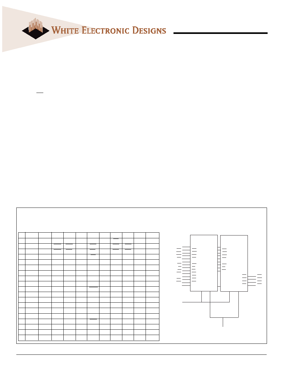
FIG. 1 PIN CONFIGURATION
BLOCK DIAGRAM
(TOP VIEW)
Address Bus
(A0-A19)
D0 - D35
D36 - D71
DQ0 - DQ71
1M x 36
CLK
CKE
ADV
LBO
CS1
CS2
OE
WE
BWA
BWB
BWC
BWD
ZZ
CLK
CKE
ADV
LBO
CS1
CS2
OE
WE
BWE
BWF
BWG
BWH
ZZ
CLK
CKE
ADV
LBO
CS1
CS2
OE
WE
ZZ
BWA
BWB
BWC
BWD
BWA
BWB
BWC
BWD
FEATURES
n Fast clock speed: 225, 200, 166 and 150MHz
n Fast access times: 2.8, 3.0, 3.5 and 3.8ns
n Fast OE access times: 2.8, 3.0, 3.5 and 3.8ns
n Separate Core and I/O Power Supply
n Snooze Mode for reduced-standby power
n Individual Byte Write control
n Clock-controlled and registered addresses,
data I/Os and control signals
n Burst control (interleaved or linear burst)
n Packaging:
209-bump BGA package, JEDEC Pin Definition
n Low capacitive bus loading
Preliminary*
* This data sheet describes a product that may not be fully qualified or
characterized and is subject to change without notice.
12
3
4
5
6
7
8
9
10
11
A DQG
DQG
ACS2
A
ADV
A
CS2
ADQB DQB
B DQG
DQG BWC BWG
NC
WE
A
BWB BWF DQB DQB
C DQG
DQG BWH BWD
NC CS1
NC BWE BWA DQB DQB
D DQG
DQG
VSS
NC
OE
NC
VSS DQB DQB
E DQPG DQPC VDDQ VDDQ VDD VDD
VDD VDDQ VDDQ DQPF DQPB
F DQC
DQC
VSS
NC
VSS VSS
VSS DQF DQF
G DQC
DQC VDDQ VDDQ VDD NC
VDD VDDQ VDDQ DQF DQF
H DQC
DQC
VSS
NC
VSS VSS
VSS DQF DQF
J
DQC
DQC VDDQ VDDQ VDD NC
VDD VDDQ VDDQ DQF DQF
K
NC
CLK
NC
VSS CKE
VSS
NC
L DQH
DQH VDDQ VDDQ VDD NC
VDD VDDQ VDDQ DQA DQA
M DQH
DQH
VSS
NC
VSS VSS
VSS DQA DQA
N DQH
DQH VDDQ VDDQ VDD NC
VDD VDDQ VDDQ DQA DQA
P DQH
DQH
VSS
ZZ
VSS VSS
VSS DQA DQA
R DQPD DQPH VDDQ VDDQ VDD VDD
VDD VDDQ VDDQ DQPA DQPE
T DQD
DQD
VSS
NC
NC LBO
NC
VSS DQE DQE
U DQD
DQD
NC
A
A19
AA
A
NC DQE DQE
V DQD
DQD
AA
A
A1
AA
A
DQE DQE
W DQD
DQD RFU RFU
A
A0
A
RFU RFU DQE DQE
January 2003 Rev. 1
ECO #15889
相关PDF资料 |
PDF描述 |
|---|---|
| W2Z512K72SJ35ES | 512K X 72 MULTI DEVICE SRAM MODULE, 3.5 ns, PBGA209 |
| W332M64V-125BC | 32M X 64 SYNCHRONOUS DRAM, 6 ns, PBGA219 |
| W332M64V-100BI | 32M X 64 SYNCHRONOUS DRAM, 7 ns, PBGA219 |
| W332M72V-100SBM | 32M X 72 SYNCHRONOUS DRAM, 7 ns, PBGA208 |
| W332M72V-125SBC | 32M X 72 SYNCHRONOUS DRAM, 6 ns, PBGA208 |
相关代理商/技术参数 |
参数描述 |
|---|---|
| W-3 | 功能描述:保险丝 125V 3A Fast Acting Plug Fuse RoHS:否 制造商:Littelfuse 产品:Surface Mount Fuses 电流额定值:0.5 A 电压额定值:600 V 保险丝类型:Fast Acting 保险丝大小/组:Nano 尺寸:12.1 mm L x 4.5 mm W 安装风格: 端接类型:SMD/SMT 系列:485 |
| W30 | 功能描述:电线导管 Pressure-Type Wire Connector RoHS:否 制造商:Panduit 类型:Slotted SideWall Open finger design wiring cut 材料:Polypropylene 颜色:Light Gray 大小: 最大光束直径: 抗拉强度: 外部导管宽度:25 mm 外部导管高度:25 mm |
| W-30 | 制造商:Cooper Bussmann 功能描述:Fuse Plug 30A 125V Fast 2-Pin Plug Threaded Socket |
| W30_11 | 制造商:WELWYN 制造商全称:Welwyn Components Limited 功能描述:Cement Coated Wirewound Resistors |
| W3000 | 功能描述:天线 2.4GHz ceramic antenna RoHS:否 制造商:Molex 技术类型:Cellular Antenna 频率: 带宽: 尺寸:106.7 mm L x 13 mm W |
发布紧急采购,3分钟左右您将得到回复。