- 您现在的位置:买卖IC网 > PDF目录68450 > W3E32M64SA-333BC (MICROSEMI CORP-PMG MICROELECTRONICS) 32M X 64 DDR DRAM, 0.7 ns, PBGA219 PDF资料下载
参数资料
| 型号: | W3E32M64SA-333BC |
| 厂商: | MICROSEMI CORP-PMG MICROELECTRONICS |
| 元件分类: | DRAM |
| 英文描述: | 32M X 64 DDR DRAM, 0.7 ns, PBGA219 |
| 封装: | 25 X 25 MM, PLASTIC, BGA-219 |
| 文件页数: | 10/17页 |
| 文件大小: | 701K |
| 代理商: | W3E32M64SA-333BC |
W3E32M64SA-XBX
2
White Electronic Designs Corporation (602) 437-1520 www.whiteedc.com
White Electronic Designs
December 2007
Rev. 1
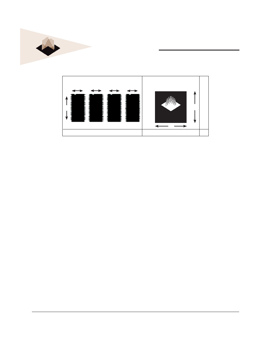
Area
4 x 265mm2 = 1060mm2
625mm2
41%
S
A
V
I
N
G
S
Actual Size
W3E32M64S-XBX
25
White Electronic Designs
W3E32M64S-XBX
25
TSOP Approach (mm)
22.3
11.9
66
TSOP
66
TSOP
66
TSOP
66
TSOP
11.9
DENSITY COMPARISONS
edges of DQS, as well as to both edges of CK.
Read and write accesses to the DDR SDRAM are burst
oriented; accesses start at a selected location and continue
for a programmed number of locations in a programmed
sequence. Accesses begin with the registration of an
ACTIVE command, which is then followed by a READ or
WRITE command. The address bits registered coincident
with the ACTIVE command are used to select the bank
and row to be accessed. The address bits registered
coincident with the READ or WRITE command are used
to select the bank and the starting column location for the
burst access.
The DDR SDRAM provides for programmable READ
or WRITE burst lengths of 2, 4, or 8 locations. An auto
precharge function may be enabled to provide a self-
timed row precharge that is initiated at the end of the
burst access.
The pipelined, multibank architecture of DDR SDRAMs
allows for concurrent operation, thereby providing high
effective bandwidth by hiding row precharge and activation
time.
An auto refresh mode is provided, along with a power-
saving power-down mode.
FUNCTIONAL DESCRIPTION
Read and write accesses to the DDR SDRAM are burst
oriented; accesses start at a selected location and continue
for a programmed number of locations in a programmed
sequence. Accesses begin with the registration of an
ACTIVE command which is then followed by a READ or
WRITE command. The address bits registered coincident
with the ACTIVE command are used to select the bank and
row to be accessed (BA0 and BA1 select the bank, A0-12
select the row). The address bits registered coincident
with the READ or WRITE command are used to select the
starting column location for the burst access.
Prior to normal operation, the DDR SDRAM must be
initialized. The following sections provide detailed
information covering device initialization, register denition,
command descriptions and device operation.
INITIALIZATION
DDR SDRAMs must be powered up and initialized in a
predened manner. Operational procedures other than
those specied may result in undened operation. Power
must rst be applied to VCC and VCCQ simultaneously, and
then to VREF (and to the system VTT). VTT must be applied
after VCCQ to avoid device latch-up, which may cause
permanent damage to the device. VREF can be applied any
time after VCCQ but is expected to be nominally coincident
with VTT. Except for CKE, inputs are not recognized as valid
until after VREF is applied. CKE is an SSTL_2 input but will
相关PDF资料 |
PDF描述 |
|---|---|
| W3E32M64SA-333BM | 32M X 64 DDR DRAM, 0.7 ns, PBGA219 |
| W3E32M64SA-333BI | 32M X 64 DDR DRAM, 0.7 ns, PBGA219 |
| W3E32M72S-200SBM | 32M X 72 DDR DRAM, 0.8 ns, PBGA208 |
| W3E32M72S-200SBM | 32M X 72 DDR DRAM, 0.8 ns, PBGA208 |
| W3E32M72S-333SBM | 32M X 72 DDR DRAM, 0.7 ns, PBGA208 |
相关代理商/技术参数 |
参数描述 |
|---|---|
| W3E32M64SA-333BI | 制造商:White Electronic Designs 功能描述:FOUR-PORT, MIXED SIGNAL, HIGH-VOLTAGE HIGH POWER OVER ET 制造商:Microsemi Corporation 功能描述:32M X 64 DDR, 2.5V, 333 MHZ, 219 PBGA, INDUSTRIAL TEMP. - Bulk 制造商:Microsemi Corporation 功能描述:SDRAM MEMORY |
| W3E32M64SA-333BM | 制造商:Microsemi Corporation 功能描述:32M X 64 DDR, 2.5V, 333 MHZ, 219 PBGA, MIL-TEMP. - Bulk |
| W3E32M64S-XBX | 制造商:WEDC 制造商全称:White Electronic Designs Corporation 功能描述:32Mx64 DDR SDRAM |
| W3E32M64S-XSBX | 制造商:WEDC 制造商全称:White Electronic Designs Corporation 功能描述:32Mx64 DDR SDRAM |
| W3E32M72S-200BC | 制造商:Microsemi Corporation 功能描述:32M X 72 DDR, 2.5V, 200 MHZ, 219 PBGA, COMMERCIAL TEMP. - Bulk |
发布紧急采购,3分钟左右您将得到回复。