- 您现在的位置:买卖IC网 > PDF目录276857 > W3EG7232S262AD4IS (MICROSEMI CORP-PMG MICROELECTRONICS) 32M X 72 DDR DRAM MODULE, 0.75 ns, DMA200 PDF资料下载
参数资料
| 型号: | W3EG7232S262AD4IS |
| 厂商: | MICROSEMI CORP-PMG MICROELECTRONICS |
| 元件分类: | DRAM |
| 英文描述: | 32M X 72 DDR DRAM MODULE, 0.75 ns, DMA200 |
| 封装: | SODIMM-200 |
| 文件页数: | 14/14页 |
| 文件大小: | 324K |
| 代理商: | W3EG7232S262AD4IS |
9
White Electronic Designs Corporation (602) 437-1520 www.whiteedc.com
White Electronic Designs
W3EG7232S-xAD4
-xBD4
March 2007
Rev. 5
Notes
1.
All voltages referenced to VSS.
2.
Tests for AC timing, IDD, and electrical AC and DC characteristics may be
conducted at nominal reference/supply voltage levels, but the related specications
and device operation are guaranteed for the full voltage range specied.
3.
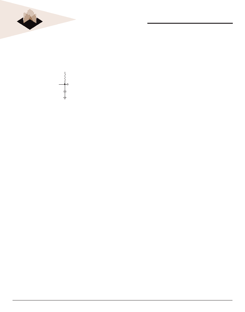
Outputs measured with equivalent load:
Output
(V
(VOUT
OUT
)
Reference
Point
50Ω
VTT
TT
30pF
4.
AC timing and IDD tests may use a VIL-to-VIH swing of up to 1.5V in the test
environment, but input timing is still referenced to VREF (or to the crossing point for
CK/CK#), and parameter specications are guaranteed for the specied AC input
levels under normal use conditions. The mini-mum slew rate for the input signals
used to test the device is 1V/ns in the range between VIL (AC) and VIH (AC).
5.
The AC and DC input level specications are as dened in the SSTL_2 Standard
(i.e., the receiver will effectively switch as a result of the signal crossing the AC
input level, and will remain in that state as long as the signal does not ring back
above [below] the DC input LOW [HIGH] level).
6.
VREF is expected to equal VCCQ/2 of the transmitting device and to track variations
in the DC level of the same. Peak-to-peak noise (non-common mode) on Vref may
not exceed ±2 percent of the DC value. Thus, from VCCQ/2, Vref is allowed ±25mV
for DC error and an additional ±25mV for AC noise. This measurement is to be
taken at the nearest VREF bypass capacitor.
7.
VTT is not applied directly to the device. VTT is a system supply for signal
termination resistors, is expected to be set equal to VREF and must track variations
in the DC level of VREF.
8.
IDD is dependent on output loading and cycle rates. Specied values are obtained
with mini-mum cycle time at CL = 2 for 262 and 202, CL = 2.5 for 335 and 265 with
the outputs open.
9.
Enables on-chip refresh and address counters.
10. IDD specications are tested after the device is properly initialized, and is averaged
at the dened cycle rate.
11. This parameter is sampled. VCC = +2.5V ±0.2V, VCCQ = +2.5V ±0.2V, VREF = VSS,
f = 100 MHz, TA = 25°C, VOUT(DC) = VCCQ/2, VOUT (peak to peak) = 0.2V. DM input
is grouped with I/O pins, reecting the fact that they are matched in loading.
12. For slew rates < 1 V/ns and ≥ to 0.5 Vns. If the slew rate is < 0.5V/ns, timing must
be derated: tIS has an additional 50ps per each 100 mV/ns reduction in slew
rate from 500 mV/ns, while tIH is unaffected. If the slew rate exceeds 4.5 V/ns,
functionality is uncertain. For 335, slew rates must be 0.5 V/ns.
13. The CK/CK# input reference level (for timing referenced to CK/CK#) is the point at
which CK and CK# cross; the input reference level for signals other than CK/CK# is
VREF.
14. Inputs are not recognized as valid until VREF stabilizes. Exception: during the period
before VREF stabilizes, CKE < 0.3 x VCCQ is recognized as LOW.
15. The output timing reference level, as measured at the timing reference point
indicated in Note 3, is VTT.
16. tHZ and tLZ transitions occur in the same access time windows as data valid
transitions. These parameters are not referenced to a specic voltage level, but
specify when the device output is no longer driving (HZ) or begins driving (LZ).
17. The intent of the Don’t Care state after completion of the postamble is the DQS-
driven signal should either be high, low, or high-Z and that any signal transition
within the input switching region must follow valid input requirements. That is, if
DQS transitions high [above VIHDC (MIN)] then it must not transition low (below
VIHDC) prior to tDQSH (MIN).
18. This is not a device limit. The device will operate with a negative value, but system
performance could be degraded due to bus turnaround.
19. It is recommended that DQS be valid (HIGH or LOW) on or before the WRITE
command. The case shown (DQS going from High-Z to logic LOW) applies when
no WRITEs were previously in progress on the bus. If a previous WRITE was in
progress, DQS could be HIGH during this time, depending on tDQSS.
20. MIN (tRC or tRFC) for IDD measurements is the smallest multiple of tCK that meets
the minimum absolute value for the respective parameter. tRAS (MAX) for IDD
measurements is the largest multiple of tCK that meets the maximum absolute value
for tRAS.
21. The refresh period 64ms. This equates to an average refresh rate of 7.8251μs.
However, an AUTO REFRESH command must be asserted at least once every
70.3μs; burst refreshing or posting by the DRAM controller greater than eight
refresh cycles is not allowed.
22. The valid data window is derived by achieving other specications: tHP (tCK/2), tDQSQ,
and tQH (tQH = tHP - tQHS). The data valid window derates in direct porportion with
the clock duty cycle and a practical data valid window can be derived, as shown in
Figure 7, Derating Data Valid Window. The clock is allowed a maximum duty cycle
variation of 45/55, beyond which functionality is uncertain. The data valid window
derating curves are provided below for duty cycles ranging between 50/50 and
45/55.
23. Each byte lane has a corresponding DQS.
24. This limit is actually a nominal value and does not result in a fail value. CKE is
HIGH during REFRESH command period (tRFC [MIN]) else CKE is LOW (i.e., during
standby).
25. To maintain a valid level, the transitioning edge of the input must:
a. Sustain a constant slew rate from the current AC level through to the target AC
level, VIL (AC) or VIH (AC).
b. Reach at least the target AC level.
c. After the AC target level is reached, continue to maintain at least the target DC
level, VIL (DC) or VIH (DC).
26. JEDEC species CK and CK# input slew rate must be ≤ 1V/ns (2V/ns
differentially).
27. DQ and DM input slew rates must not deviate from DQS by more than 10 percent.
If the DQ/DM/DQS slew rate is less than 0.5 V/ns, timing must be derated: 50ps
must be added to tDS and tDH for each 100 mv/ns reduction in slew rate. If slew rate
exceeds 4 V/ns, functionality is uncertain. For 335, slew rates must be ≥ 0.5 V/ns.
28. VCC must not vary more than 4 percent if CKE is not active while any bank is active.
29. The clock is allowed up to ±150ps of jitter. Each timing parameter is allowed to vary
by the same amount.
30. tHP min is the lesser of tCL minimum and tCH minimum actually applied to the device
CK and CK# inputs, collectively during bank active.
31. READs and WRITEs with auto precharge are not allowed to be issued until
tRAS(min) can be satised prior to the internal precharge command being issued.
32. Any positive glitch must be less than 1/3 of the clock and not more than +400mV or
2.9V, whichever is less. Any negative glitch must be less than 1/3 of the clock cycle
and not exceed either - 300mV or 2.2V, whichever is more positive.
33. The voltage levels used are derived from a mini-mum VCC level and the referenced
test load. In practice, the voltage levels obtained from a properly terminated bus will
provide signicantly different voltage values.
相关PDF资料 |
PDF描述 |
|---|---|
| W3EG7232S335BD4ISG | 32M X 72 DDR DRAM MODULE, 0.7 ns, DMA200 |
| W3H128M64E2-400SBC | DDR DRAM, PBGA208 |
| W3HG264M72EER806AD7MG | 128M X 72 DDR DRAM MODULE, DMA244 |
| W7NCF01GH21ISBCG | 64M X 16 FLASH 3.3V PROM CARD, 150 ns, UUC |
| W7NCF256H30IS7DG | 16M X 16 FLASH 3.3V PROM CARD, 150 ns, UUC |
相关代理商/技术参数 |
参数描述 |
|---|---|
| W3EG7232S262AD4-X | 制造商:WEDC 制造商全称:White Electronic Designs Corporation 功能描述:256MB - 32Mx72 DDR SDRAM UNBUFFERED w/PLL |
| W3EG7232S262BD4-X | 制造商:WEDC 制造商全称:White Electronic Designs Corporation 功能描述:256MB - 32Mx72 DDR SDRAM UNBUFFERED w/PLL |
| W3EG7232S265AD4-X | 制造商:WEDC 制造商全称:White Electronic Designs Corporation 功能描述:256MB - 32Mx72 DDR SDRAM UNBUFFERED w/PLL |
| W3EG7232S265BD4-X | 制造商:WEDC 制造商全称:White Electronic Designs Corporation 功能描述:256MB - 32Mx72 DDR SDRAM UNBUFFERED w/PLL |
| W3EG7232S335AD4-X | 制造商:WEDC 制造商全称:White Electronic Designs Corporation 功能描述:256MB - 32Mx72 DDR SDRAM UNBUFFERED w/PLL |
发布紧急采购,3分钟左右您将得到回复。