- 您现在的位置:买卖IC网 > PDF目录245665 > W3EG7262S262JD3 (WHITE ELECTRONIC DESIGNS CORP) DDR DRAM MODULE, DMA184 PDF资料下载
参数资料
| 型号: | W3EG7262S262JD3 |
| 厂商: | WHITE ELECTRONIC DESIGNS CORP |
| 元件分类: | DRAM |
| 英文描述: | DDR DRAM MODULE, DMA184 |
| 封装: | ROHS COMPLIANT, DIMM-184 |
| 文件页数: | 8/12页 |
| 文件大小: | 279K |
| 代理商: | W3EG7262S262JD3 |
W3EG7262S-D3
-JD3
5
White Electronic Designs Corporation (602) 437-1520 www.whiteedc.com
White Electronic Designs
May 2005
Rev. 3
PRELIMINARY
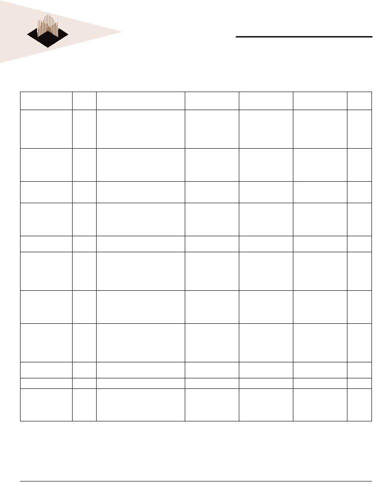
IDD SPECIFICATIONS AND TEST CONDITIONS
Recommended operating conditions, 0°C TA 70°C, VCCQ = 2.5V ± 0.2V, VCC = 2.5V ± 0.2V
Includes DDR SDRAM component only
Parameter
Symbol Conditions
DDR266@CL=2.0
Max
DDR266@CL=2.5
Max
DDR200@CL=2
Max
Units
Operating Current
IDD0
One device bank; Active - Precharge;
tRC=tRC (MIN); tCK=tCK (MIN); DQ,DM
and DQS inputs changing once per
clock cycle; Address and control
inputs changing once every two
cycles.
TBD
1845
mA
Operating Current
IDD1
One device bank; Active-Read-
Precharge Burst = 2; tRC=tRC (MIN);
tCK=tCK (MIN); lOUT = 0mA; Address
and control inputs changing once per
clock cycle.
TBD
2205
mA
Precharge Power-
Down Standby
Current
IDD2P
All device banks idle; Power-down
mode; tCK=tCK (MIN); CKE=(low)
TBD
72
rnA
Idle Standby Current
IDD2F
CS# = High; All device banks idle;
tCK=tCK (MIN); CKE = high; Address
and other control inputs changing
once per clock cycle. VIN = VREF for
DQ, DQS and DM.
TBD
810
mA
Active Power-Down
Standby Current
IDD3P
One device bank active; Power-Down
mode; tCK (MIN); CKE=(low)
TBD
450
mA
Active Standby
Current
IDD3N
CS# = High; CKE = High; One device
bank; Active-Precharge; tRC=tRAS
(MAX); tCK=tCK (MIN); DQ, DM and
DQS inputs changing twice per clock
cycle; Address and other control
inputs changing once per clock cycle.
TBD
900
mA
Operating Current
IDD4R
Burst = 2; Reads; Continuous burst;
One device bank active; Address
and control inputs changing once
per clock cycle; TCK= TCK (MIN); lOUT
= 0mA.
TBD
2250
mA
Operating Current
IDD4W
Burst = 2; Writes; Continuous burst;
One device bank active; Address
and control inputs changing once per
clock cycle; tCK=tCK (MIN); DQ,DM
and DQS inputs changing once per
clock cycle.
TBD
2115
rnA
Auto Refresh
Current
IDD5
tRC = tRC (MIN)
TBD
3015
mA
Self Refresh Current
IDD6
CKE 0.2V
TBD
72
mA
Operating Current
IDD7A
Four bank interleaving Reads (BL=4)
with auto precharge with tRC=tRC
(MIN); tCK=tCK (MIN); Address and
control inputs change only during
Active Read or Write commands.
TBD
4050
mA
相关PDF资料 |
PDF描述 |
|---|---|
| W7NCF08GH10CS4BM1G | FLASH 3.3V PROM MODULE, XMA50 |
| W7NCF08GH10CS7JM1G | FLASH 3.3V PROM MODULE, XMA50 |
| W7NCF08GH10CSA4JM1G | FLASH 3.3V PROM MODULE, XMA50 |
| W7NCF08GH10IS2AM1G | FLASH 3.3V PROM MODULE, XMA50 |
| W7NCF08GH10ISA5FM1G | FLASH 3.3V PROM MODULE, XMA50 |
相关代理商/技术参数 |
参数描述 |
|---|---|
| W3EG7262S265D3 | 制造商:WEDC 制造商全称:White Electronic Designs Corporation 功能描述:512MB - 2X32Mx72 DDR SDRAM UNBUFFERED |
| W3EG7262S265JD3 | 制造商:WEDC 制造商全称:White Electronic Designs Corporation 功能描述:512MB - 2X32Mx72 DDR SDRAM UNBUFFERED |
| W3EG7262S-D3 | 制造商:WEDC 制造商全称:White Electronic Designs Corporation 功能描述:512MB - 2X32Mx72 DDR SDRAM UNBUFFERED |
| W3EG7262S-JD3 | 制造商:WEDC 制造商全称:White Electronic Designs Corporation 功能描述:512MB - 2X32Mx72 DDR SDRAM UNBUFFERED |
| W3EG7263S202AJD3 | 制造商:WEDC 制造商全称:White Electronic Designs Corporation 功能描述:512MB- 64Mx72 DDR SDRAM REGISTERED w/PLL |
发布紧急采购,3分钟左右您将得到回复。