- 您现在的位置:买卖IC网 > PDF目录68459 > W3HG64M72EER806PD4MG (MICROSEMI CORP-PMG MICROELECTRONICS) 64M X 72 DDR DRAM MODULE, DMA200 PDF资料下载
参数资料
| 型号: | W3HG64M72EER806PD4MG |
| 厂商: | MICROSEMI CORP-PMG MICROELECTRONICS |
| 元件分类: | DRAM |
| 英文描述: | 64M X 72 DDR DRAM MODULE, DMA200 |
| 封装: | ROHS COMPLIANT, SO-RDIMM-200 |
| 文件页数: | 13/13页 |
| 文件大小: | 249K |
| 代理商: | W3HG64M72EER806PD4MG |
W3HG64M72EER-PD4
February 2007
Rev. 0
9
White Electronic Designs Corporation (602) 437-1520 www.whiteedc.com
White Electronic Designs
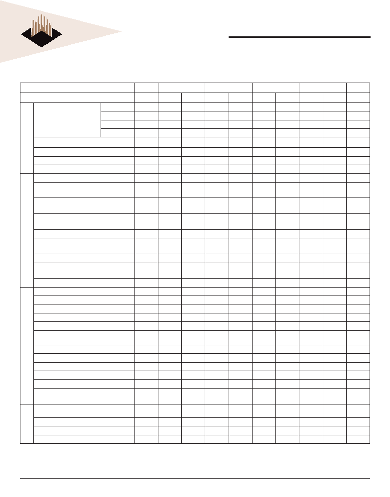
DDR2 SDRAM COMPONT AC TIMING PARAMETERS & SPECIFICATIONS
VCC = +1.8V ± 0.1V
AC CHARACTERISTICS
806
665
534
403
PARAMETER
SYMBOL
MIN
MAX
MIN
MAX
MIN
MAX
MIN
MAX
UNIT
Clock
Clock cycle time
CL = 6
tCK (6)
TBD
ps
CL = 5
tCK (5)
TBD
3,000
8,000
ps
CL = 4
tCK (4)
TBD
3,750
8,000
3,750
8,000
5,000
8,000
ps
CL = 3
tCK (3)
TBD
5,000
8,000
5,000
8,000
5,000
8,000
ps
CK high-level width
tCH
TBD
0.45
0.55
0.45
0.55
0.45
0.55
tCK
CK low-level width
tCL
TBD
0.45
0.55
0.45
0.55
0.45
0.55
tCK
Half clock period
tHP
TBD
MIN
(tCH,tCL)
MIN
(tCH,tCL)
MIN
(tCH,tCL)ps
Clock jitter
tJIT
TBD
-125
125
-125
125
-125
125
ps
Data
DQ output access time from CK/CK#
tAC
TBD
-450
+450
-500
+500
-600
+600
ps
Data-out high-impedance window from
CK/CK#
tHZ
TBD
tAC(MAX)
ps
Data-out low-impedance window from
CK/CK#
tLZ
TBD
tAC(MIN)
tAC(MAX)
tAC(MIN)
tAC(MAX)
tAC(MIN)
tAC(MAX)
ps
DQ and DM input setup time relative to
DQS
tDS
TBD
100
150
DQ and DM input hold time relative to DQS
tDH
TBD
225
275
DQ and DM input pulse width (for each
input)
tDIPW
TBD
0.35
tCK
Data hold skew factor
tQHS
TBD
340
400
450
ps
DQ - DQS hold, DQS to rst DQ to go
nonvalid, per access
tQH
TBD
tHP - tQHS
ps
Data valid output window (DVW)
tDVW
TBD
tQH - tDQSQ
ns
Data
Strobe
DQS input high pulse width
tDQSH
TBD
0.35
tCK
DQS input low pulse width
tDQSL
TBD
0.35
tCK
DQS output access time from CK/CK#
tDQSCK
TBD
-400
+400
-450
+450
-500
+500
ps
DQS falling edge to CK rising - setup time
tDSS
TBD
0.2
tCK
DQS falling edge from CK rising - hold time
tDSH
TBD
0.2
tCK
DQS - DQ skew, DQS to last DQ valid, per
group, per access
tDQSQ
TBD
240
300
350
ps
DQS read preamble
tRPRE
TBD
0.9
1.1
0.9
1.1
0.9
1.1
tCK
DQS read postamble
tRPST
TBD
0.4
0.6
0.4
0.6
0.4
0.6
tCK
DQS write preamble setup time
tWPRES
TBD
000
ps
DQS write preamble
tWPRE
TBD
0.35
tCK
DQS write postamble
tWPST
TBD
0.4
0.6
0.4
0.6
0.4
0.6
tCK
Write command to rst DQS latching
transition
tDQSS
TBD
WL-
0.25
WL+
0.25
WL-
0.25
WL+
0.25
WL-
0.25
WL+
0.25
tCK
Address and control input pulse width for
each input
tIPW
TBD
0.6
tCK
Address and control input setup time
tIS
TBD
200
250
350
ps
Address and control input hold time
tIH
TBD
275
375
475
ps
Address and control input hold time
tCCD
TBD
222
tCK
* AC specication is based on
SAMSUNG components. Other DRAM manufactures specication may be different.
Continued on next page
相关PDF资料 |
PDF描述 |
|---|---|
| W3HG64M72EER534PD4MG | 64M X 72 DDR DRAM MODULE, 0.5 ns, DMA200 |
| W3HG64M72EEU806PD4GG | 64M X 72 DDR DRAM MODULE, DMA200 |
| W45B010P | 1M X 1 FLASH 2.7V PROM, PQCC32 |
| W49F002U-90BN | 256K X 8 FLASH 5V PROM, 90 ns, PDIP32 |
| W49F002UT12N | 256K X 8 FLASH 5V PROM, 120 ns, PDSO32 |
相关代理商/技术参数 |
参数描述 |
|---|---|
| W3HG64M72EER-AD7 | 制造商:WEDC 制造商全称:White Electronic Designs Corporation 功能描述:512MB - 64Mx72 DDR2 SDRAM REGISTERED, w/PLL, VLP Mini-DIMM |
| W3J128M72G-1066PBI | 制造商:Microsemi Corporation 功能描述:DRAM MODULE DDR3 SDRAM 9G-BIT - Bulk 制造商:Microsemi Corporation 功能描述:SDRAM MEMORY |
| W3J128M72G-800PBI | 制造商:Microsemi Corporation 功能描述:SDRAM MEMORY |
| W3J512M72G-1333PBI | 制造商:Microsemi Corporation 功能描述:512MX72 DDR3, 1333MHZ, I-TEMP OPERATING RANGE - Bulk |
| W3J512M72G-800PBI | 制造商:Microsemi Corporation 功能描述:SDRAM MEMORY |
发布紧急采购,3分钟左右您将得到回复。