- 您现在的位置:买卖IC网 > PDF目录140369 > W78M64V-70SBM (WHITE ELECTRONIC DESIGNS CORP) 8M X 64 FLASH 3.3V PROM MODULE, 70 ns, PBGA159 PDF资料下载
参数资料
| 型号: | W78M64V-70SBM |
| 厂商: | WHITE ELECTRONIC DESIGNS CORP |
| 元件分类: | PROM |
| 英文描述: | 8M X 64 FLASH 3.3V PROM MODULE, 70 ns, PBGA159 |
| 封装: | 13 X 22 MM, 1.27 MM PITCH, PLASTIC, BGA-159 |
| 文件页数: | 34/54页 |
| 文件大小: | 1349K |
| 代理商: | W78M64V-70SBM |
第1页第2页第3页第4页第5页第6页第7页第8页第9页第10页第11页第12页第13页第14页第15页第16页第17页第18页第19页第20页第21页第22页第23页第24页第25页第26页第27页第28页第29页第30页第31页第32页第33页当前第34页第35页第36页第37页第38页第39页第40页第41页第42页第43页第44页第45页第46页第47页第48页第49页第50页第51页第52页第53页第54页
4
White Electronic Designs Corporation (602) 437-1520 www.whiteedc.com
White Electronic Designs
W78M64V-XSBX
July 2006
Rev. 4
White Electronic Designs Corp. reserves the right to change products or specications without notice.
DEVICE BUS OPERATIONS
This section describes the requirements and use of the
device bus operations, which are initiated through the
internal command register. The command register itself
does not occupy any addressable memory location. The
register is a latch used to store the commands, along with
the address and data information needed to execute the
command. The contents of the register serve as inputs
to the internal state machine. The state machine outputs
dictate the function of the device. Table 1 lists the device
bus operations, the inputs and control levels they require,
and the resulting output. The following subsections describe
each of these operations in further detail.
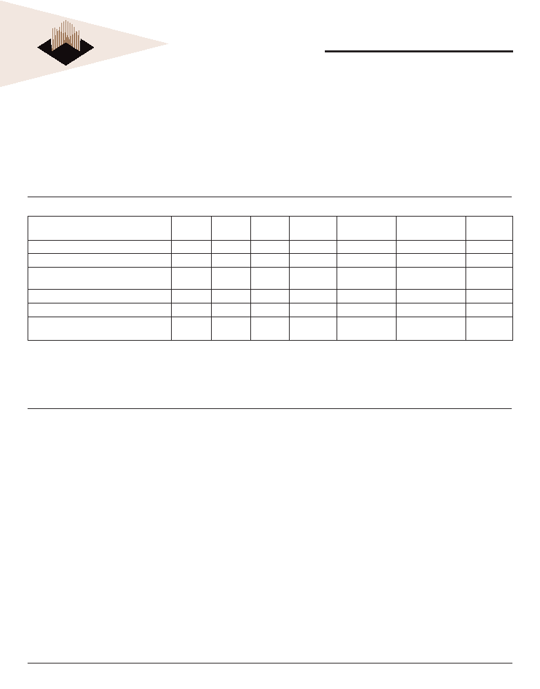
TABLE 1. DEVICE BUS OPERATION3
Operation
CS#
OE#
WE#
RESET#
WP#/ACC
Addresses
(A22-A0)
DQ15-DQ0
Read
LL
H
X
AIN
DOUT
Write
LH
L
H
X
AIN
DIN
Standby
VIO±
0.3 V
XX
VIO ±
0.3 V
X (Note 2)
X
High-Z
Output Disable
L
H
X
High-Z
Reset
X
L
X
High-Z
Temporary Sector Unprotect (High
Voltage
XX
X
VID
XAIN
DIN
Legend: L = Logic Low = VIL, H = Logic High = VIH, VID = 11.5-12.5 V, VHH = 8.5-9.5 V, X = Don’t Care, SA = Sector Address, AIN = Address In, DIN = Data In,
DOUT = Data Out
Notes:
1.
The sector protect and sector unprotect functions may also be Implemented via programming equipment. See the High Voltage Sector Protection section.
2.
WP#/ACC must be high when writing to sectors 0, 1, 268, or 269.
3.
For each chip
REQUIREMENTS FOR READING
ARRAY DATA
To read array data from the outputs, the system must drive
the OE# and appropriate CS# pins to VIL. CS# is the power
control. OE# is the output control and gates array data to
the output pins. WE# should remain at VIH.
The internal state machine is set for reading array data upon
device power-up, or after a hardware reset. This ensures
that no spurious alteration of the memory content occurs
during the power transition. No command is necessary in
this mode to obtain array data. Standard microprocessor
read cycles that assert valid addresses on the device
address inputs produce valid data on the device data
outputs. Each bank remains enabled for read access until
the command register contents are altered.
Refer to theAC Characteristics table for timing specications
and to Figure 11 for the timing diagram. ICC1 in the
DC Characteristics table represents the active current
specication for reading array data.
Random Read (Non-Page Read)
Address access time (tACC) is equal to the delay from stable
addresses to valid output data. The chip enable access
time (tCS) is the delay from the stable addresses and stable
CS# to valid data at the output inputs. The output enable
access time is the delay from the falling edge of the OE#
to valid data at the output inputs (assuming the addresses
have been stable for at least tACC–tOE time).
Page Mode Read
The device is capable of fast page mode read and is
compatible with the page mode Mask ROM read operation.
This mode provides faster read access speed for random
locations within a page. Address bits A22–A3 select an 8
word page, and address bits A2–A0 select a specic word
within that page. This is an asynchronous operation with the
microprocessor supplying the specic word location.
The random or initial page access is tACC or tCS and
subsequent page read accesses (as long as the locations
specied by the microprocessor falls within that page) is
相关PDF资料 |
PDF描述 |
|---|---|
| WS128K32L-45G2TMA | 128K X 32 MULTI DEVICE SRAM MODULE, 45 ns, CQFP68 |
| WS128K32L-55G2TM | 128K X 32 MULTI DEVICE SRAM MODULE, 55 ns, CQFP68 |
| WF512K32F-60G4Q5A | 512K X 32 FLASH 5V PROM MODULE, 60 ns, CQFP68 |
| WF512K32N-60H1Q5 | 512K X 32 FLASH 5V PROM MODULE, 60 ns, CHIP66 |
| WF512K32-70G2UQ5A | 512K X 32 FLASH 5V PROM MODULE, 70 ns, CQFP68 |
相关代理商/技术参数 |
参数描述 |
|---|---|
| W78M64VP110SBM | 制造商:Microsemi Corporation 功能描述:8MX64 FLASH 3.3V PAGE MODE - Bulk |
| W78M64V-XSBX | 制造商:未知厂家 制造商全称:未知厂家 功能描述:Flash MCP |
| W78NCSX-23 | 功能描述:低信号继电器 - PCB 4PDT 3A 24VDC IND RoHS:否 制造商:NEC 触点形式:2 Form C (DPDT-BM) 触点电流额定值: 线圈电压:5 V 最大开关电流:1 A 线圈电流:1 A 线圈类型:Non-Latching 功耗:140 mW 端接类型:SMT 绝缘: 介入损耗: |
| W78PCX-1 | 制造商:Magnecraft 功能描述: |
| W78PCX-2 | 制造商:Magnecraft 功能描述: |
发布紧急采购,3分钟左右您将得到回复。