- 您现在的位置:买卖IC网 > PDF目录225537 > WB1336TX-TR Serial-Input Frequency Synthesizer PDF资料下载
参数资料
| 型号: | WB1336TX-TR |
| 英文描述: | Serial-Input Frequency Synthesizer |
| 中文描述: | 串行输入频率合成器 |
| 文件页数: | 4/10页 |
| 文件大小: | 160K |
| 代理商: | WB1336TX-TR |
WB1330
3
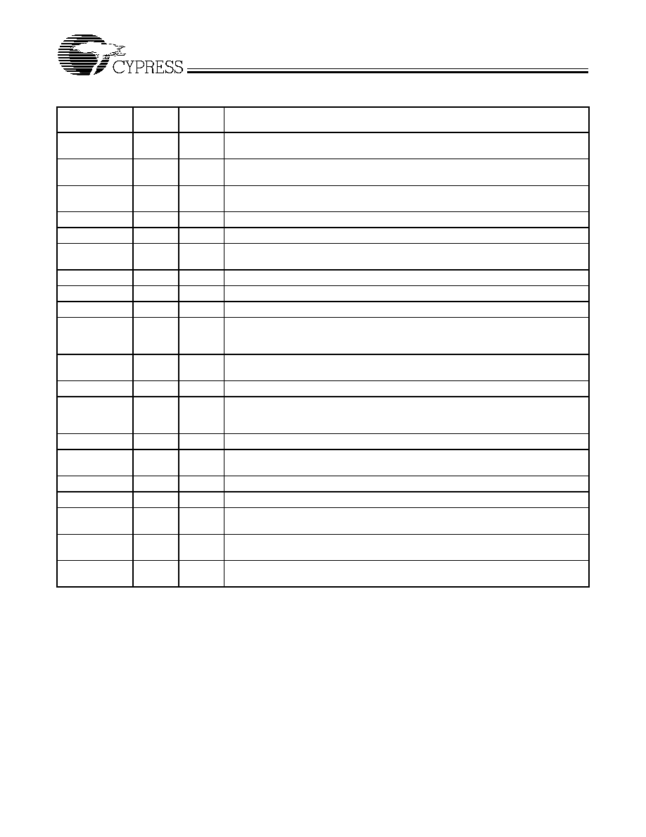
Pin Definitions
Pin Name
Pin
No.
Pin
Type
Pin Description
VCC11
P
Power Supply Connection for PLL1 and PLL2: When power is removed from both
the VCC1 and VCC2 pins, all latched data is lost.
VP12
P
PLL1 Charge Pump Rail Voltage: This voltage accommodates VCO circuits with
tuning voltages higher than the VCC of PLL1.
DOPLL1
3
O
PLL1 Charge Pump Output: The phase detector gain is IP/2π. Sense polarity can be
reversed by setting the FC bit in software (via the Shift Register).
GND
4
G
Analog and Digital Ground Connection: This pin must be grounded.
FIN15
I
Input to PLL1 Prescaler: Maximum frequency 2.5 GHz.
FIN1#
6
I
Complementary Input to PLL1 Prescaler: A bypass capacitor should be placed as
close as possible to this pin and must be connected directly to the ground plane.
GND
7
G
Analog and Digital Ground Connection: This pin must be grounded.
OSC_IN
8
I
Oscillator Input: This input has a VCC/2 threshold and CMOS logic level sensitivity.
GND
9
G
Reference Ground Connection: This pin must be grounded.
FO/LD
10
O
Lock Detect Pin of PLL1 Section: This output is HIGH when the loop is locked. It is
multiplexed to the output of the programmable counters or reference dividers in the
test program mode. (Refer to Table 3 for configuration.)
CLOCK
11
I
Data Clock Input: One bit of data is loaded into the Shift Register on the rising edge
of this signal.
DATA
12
I
Serial Data Input
LE
13
I
Load Enable: On the rising edge of this signal, the data stored in the Shift Register
is latched into the reference counter and configuration controls, PLL1 or PLL2 depend-
ing on the state of the control bits.
GND
14
G
Analog and Digital Ground Connection: This pin must be grounded.
FIN2#
15
I
Complementary Input to PLL2 Prescaler: A bypass capacitor should be placed as
close as possible to this pin and must be connected directly to the ground plane.
FIN216
I
Input to PLL2 Prescaler: Maximum frequency 600 MHz.
GND
17
G
Analog and Digital Ground Connections: This pin must be grounded.
DOPLL2
18
O
PLL2 Charge Pump Output: The phase detector gain is IP/2π. Sense polarity can be
reversed by setting the FC bit in software (via the Shift Register).
VP219
P
PLL2 Charge Pump Rail Voltage: This voltage accommodates VCO circuits with
tuning voltages higher than the VCC of PLL2.
VCC220
P
Power Supply Connections for PLL1 and PLL2: When power is removed from both
the VCC1 and VCC2 pins, all latched data is lost.
相关PDF资料 |
PDF描述 |
|---|---|
| WB1356X | Serial-Input Frequency Synthesizer |
| WB416-PQ-20 | Write Buffer |
| WB416-PQ-33 | Write Buffer |
| WB416-PQ-50 | Write Buffer |
| WB418-PQ-20 | Write Buffer |
相关代理商/技术参数 |
参数描述 |
|---|---|
| WB1356X | 制造商:未知厂家 制造商全称:未知厂家 功能描述:Serial-Input Frequency Synthesizer |
| WB13FJ | 制造商:Eaton Corporation 功能描述:SZ 1 ADV STAND-ALONE OL, 3P 120V 60HZ |
| WB14 | 功能描述:BRACKET WALL 13 SLOT RoHS:是 类别:测试设备 >> 配件 系列:- 标准包装:1 系列:Anaheim Scientific 类型:专用 附件类型:三脚架 适用于相关产品:仪表 技术规格:- 配用:BK725-ND - DATALOG HUMID/TEMP METER W/DL INBK720-ND - HUMIDITY/TEMP METER W/DUAL INPUT 其它名称:BKTRISND |
| WB1400-BTS7230 | 制造商:LISTA 功能描述:Workbench Combination 制造商:Lista International Corp 功能描述:Workbench Combination |
| WB1500-BTS7230 | 制造商:LISTA 功能描述:Workbench Combination 制造商:Lista International Corp 功能描述:Workbench Combination |
发布紧急采购,3分钟左右您将得到回复。