- 您现在的位置:买卖IC网 > PDF目录62763 > WED2DL32512V25BC 512K X 32 MULTI DEVICE SRAM MODULE, 2.5 ns, PBGA119 PDF资料下载
参数资料
| 型号: | WED2DL32512V25BC |
| 元件分类: | SRAM |
| 英文描述: | 512K X 32 MULTI DEVICE SRAM MODULE, 2.5 ns, PBGA119 |
| 封装: | PLASTIC, BGA-119 |
| 文件页数: | 1/9页 |
| 文件大小: | 143K |
| 代理商: | WED2DL32512V25BC |
1
White Electronic Designs Corporation (508) 366-5151 www.whiteedc.com
WED2DL32512V
January 2000 Rev. 0
DESCRIPTION
The WEDC SyncBurst - SRAM family employs high-speed, low-
power CMOS designs that are fabricated using an advanced CMOS
process. WEDC’s 16Mb SyncBurst SRAMs integrate two 512K x 16
SRAMs into a single BGA package to provide 512K x 32 configura-
tion. All synchronous inputs pass through registers controlled by a
positive-edge-triggered single-clock input (CLK). The synchronous
inputs include all addresses, all data inputs, active LOW chip enable
(CE), burst control input (ADSC) and byte write enables (BW0-3).
Asynchronous inputs include the output enable (OE), clock (CLK)
and snooze enable (ZZ). There is also a burst mode input (MODE)
that selects between interleaved and linear burst modes. Write cycles
can be from one to four bytes wide, as controlled by the write control
inputs. Burst operation can be initiated with the address status
controller (ADSC) input.
* This data sheet describes a product under development, not fully
characterized, and is subject to change without notice.
512Kx32 Synchronous Pipeline Burst SRAM PRELIMINARY*
FEATURES
s Fast clock speed: 200, 166, 150 & 133MHz
s Fast access times: 2.5ns, 3.5ns, 3.8ns & 4.0ns
s Fast OE access times: 2.5ns, 3.5ns, 3.8ns 4.0ns
s Single +3.3V power supply (VDD)
s Separate +3.3V or +2.5V isolated output buffer supply (VDDQ)
s Snooze Mode for reduced-power standby
s Single-cycle deselect
s Common data inputs and data outputs
s Individual Byte Write control and Global Write
s Clock-controlled and registered addresses, data I/Os and control signals
s Burst control (interleaved or linear burst)
s Packaging:
119-bump BGA package
s Low capacitive bus loading
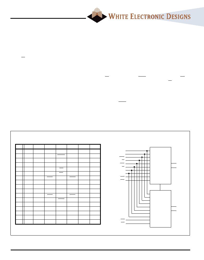
FIG. 1
BLOCK DIAGRAM
PIN CONFIGURATION
(TOP VIEW)
123
4
5
67
A
VDDQ
SA
NC
SA
VDDQ
B
NC
SA
ADSC
SA
NC
C
NC
SA
VDD
SA
NC
D
DQc
NC
VSS
NC
VSS
NC
DQb
E
DQc
VSS
CE
VSS
DQb
F
VDDQ
DQc
VSS
OE
VSS
DQb
VDDQ
G
DQc
BWc
NC
BWb
DQb
H
DQc
VSS
NC
VSS
DQb
J
VDDQ
VDD
NC
VDD
NC
VDD
VDDQ
K
DQd
VSS
CLK
VSS
DQa
L
DQd
BWd
NC
BWa
DQa
M
VDDQ
DQd
VSS
BWE
VSS
DQa
VDDQ
N
DQd
VSS
SA1
VSS
DQa
P
DQd
NC
VSS
SA0
VSS
NC
DQa
R
NC
SA
MODE
VDD
NC
SA
NC
T
NC
SA
NC
ZZ
U
VDDQ
DC
NC
VDDQ
DQb
DQa
SA
CLK
ADSC
OE
BWE
CE
MODE
ZZ
BWa
BWb
512K x 16
SSRAM
DQd
DQc
512K x 16
SSRAM
BWc
BWd
NOTE: DC = Do Not Connect
相关PDF资料 |
PDF描述 |
|---|---|
| WED3DG6318V7D2 | 16M X 64 SYNCHRONOUS DRAM MODULE, DMA168 |
| WED3DG6364V7D2 | 64M X 64 SYNCHRONOUS DRAM MODULE, DMA168 |
| WED3DG639V75D2 | 8M X 64 SYNCHRONOUS DRAM MODULE, DMA168 |
| WED3DG64128V7D1I | 128M X 64 SYNCHRONOUS DRAM MODULE, DMA144 |
| WED3DG6417V75D2I | 16M X 64 SYNCHRONOUS DRAM MODULE, DMA168 |
相关代理商/技术参数 |
参数描述 |
|---|---|
| WED2DL32512V35BC | 制造商:未知厂家 制造商全称:未知厂家 功能描述:SYNC SRAM|512KX32|CMOS|BGA|119PIN|PLASTIC |
| WED2DL32512V38BC | 制造商:WEDC 制造商全称:White Electronic Designs Corporation 功能描述:512Kx32 Synchronous Pipeline Burst SRAM |
| WED2DL32512V38BI | 制造商:未知厂家 制造商全称:未知厂家 功能描述:SYNC SRAM|512KX32|CMOS|BGA|119PIN|PLASTIC |
| WED2DL32512V40BC | 制造商:未知厂家 制造商全称:未知厂家 功能描述:SYNC SRAM|512KX32|CMOS|BGA|119PIN|PLASTIC |
| WED2DL32512V40BI | 制造商:WEDC 制造商全称:White Electronic Designs Corporation 功能描述:512Kx32 Synchronous Pipeline Burst SRAM |
发布紧急采购,3分钟左右您将得到回复。