- 您现在的位置:买卖IC网 > PDF目录276853 > WF256K16-50CC5 (MICROSEMI CORP-PMG MICROELECTRONICS) 256K X 16 FLASH 5V PROM MODULE, 50 ns, CDIP40 PDF资料下载
参数资料
| 型号: | WF256K16-50CC5 |
| 厂商: | MICROSEMI CORP-PMG MICROELECTRONICS |
| 元件分类: | PROM |
| 英文描述: | 256K X 16 FLASH 5V PROM MODULE, 50 ns, CDIP40 |
| 封装: | 0.600 INCH, SINGLE-CAVITY, SIDE BRAZED, CERAMIC, DIP-40 |
| 文件页数: | 5/11页 |
| 文件大小: | 186K |
| 代理商: | WF256K16-50CC5 |
White Microelectronics Phoenix, AZ (602) 437-1520
7
FLASH
MODULES
3
WF128K16, WF256K16-XCX5
PRINCIPLES OF OPERATION
WRITE
Device erasure and programming are accomplished via the
command register. The contents of the register serve as input
to the internal state machine. The state machine outputs
dictate the function of the device.
The command register itself does not occupy an addressable
memory location. The register is a latch used to store the
commands, along with address and data information needed to
execute the command. The command register is written by
bringing Write-Enable to a logic-low level (VIL), while Chip-Select
is low and OE is at VIH. Addresses are latched on the falling edge
of the Write-Enable while data is latched on the rising edge of the
WE pulse. Standard microprocessor write timings are used. Refer
to AC Program characteristics, Figures 4 and 7.
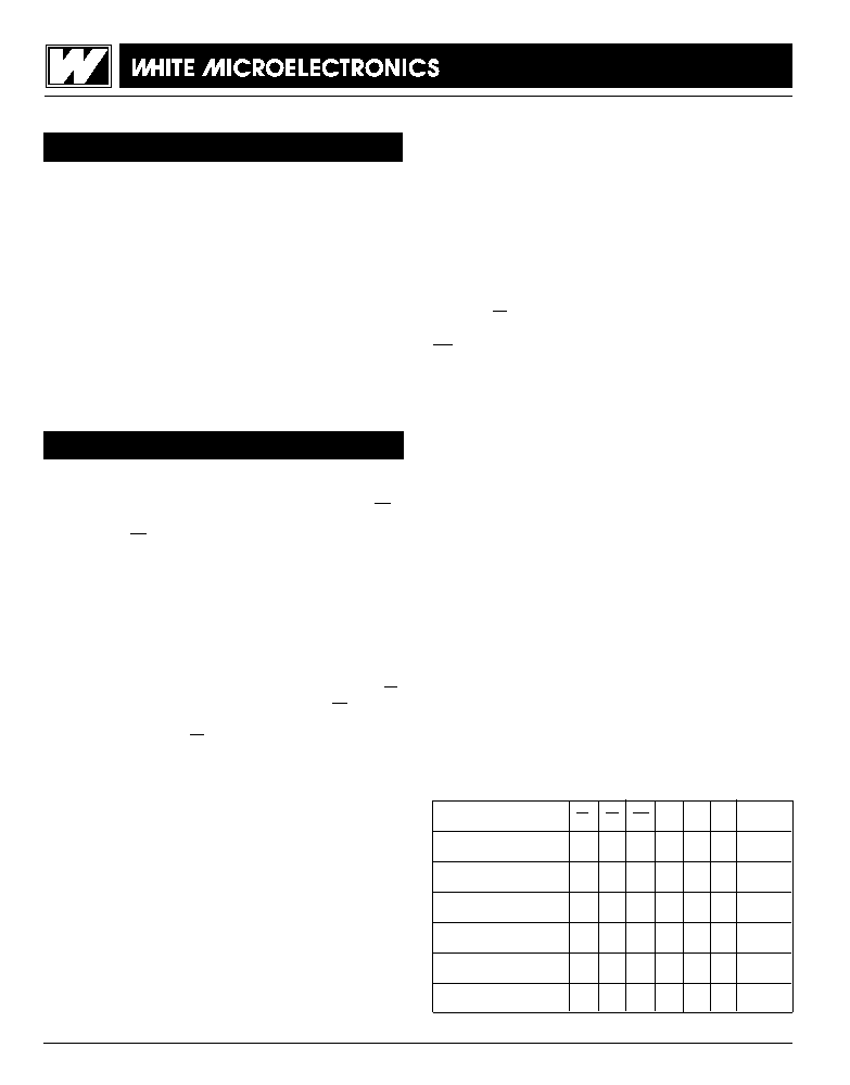
TABLE 1 - BUS OPERATIONS
Operation
CS
OE
WE
A0
A1
A9
I/O
Read
L
H
A0
A1
A9
DOUT
Standby
H
X
HIGH Z
Output Disable
L
H
X
HIGH Z
Write
L
H
L
A0
A1
A9
DIN
Enable Sector Protect
L
VID
L
XXVID
X
Verify Sector Protect
L
H
L
H
VID
Code
The following principles of operation of the WF128K16-XCX5
and WF256K16-XCX5 are applicable to each 128K x 8 memory
chip inside the MCM. Programming of the device is accom-
plished by executing the program command sequence. The
program algorithm, which is an internal algorithm, automati-
cally times the program pulse widths and verifies proper cell
margin. Sectors can be programmed and verified in less than 0.3
seconds. Erase is accomplished by executing the erase
command sequence. The erase algorithm, which is internal,
automatically preprograms the array if it is not already
programmed before executing the erase operation. During
erase, the device automatically times the erase pulse widths
and verifies proper cell margin. The entire memory is typically
erased and verified in three seconds (including pre-program-
ming).
BUS OPERATIONS
READ
The device has two control functions, both of which must be
logically active, to obtain data at the outputs. Chip-Select (CS)
is the power control and should be used for device selection.
Output-Enable (OE) is the output control and should be used to
gate data to the output pins. Figure 3 illustrates read timing
waveforms.
OUTPUT DISABLE
With Output-Enable at a logic-high level (VIH), output from the
device is disabled. Output pins are placed in a high
impedance state.
STANDBY MODE
The device has two standby modes, a CMOS standby mode (CS
input held at VCC + 0.5V), and a TTL standby mode (CS is held
VIH). In the standby mode the outputs are in a high impedance
state, independent of the OE input.
If the device is deselected during erasure or programming, the
device will draw active current until the operation is completed.
相关PDF资料 |
PDF描述 |
|---|---|
| WMS128K8-15FEC | 128K X 8 STANDARD SRAM, 15 ns, CDFP32 |
| WMS128K8-55FMA | 128K X 8 STANDARD SRAM, 55 ns, CDFP36 |
| WMS512K8-70CI | 512K X 8 STANDARD SRAM, 70 ns, CDIP32 |
| WPS512K8LC-20RJIG | 512K X 8 STANDARD SRAM, 20 ns, PDSO36 |
| WPS512K8LT-25RJMG | 512K X 8 STANDARD SRAM, 25 ns, PDSO36 |
相关代理商/技术参数 |
参数描述 |
|---|---|
| WF256K16-50CC5A | 制造商:未知厂家 制造商全称:未知厂家 功能描述:5V FLASH MODULE |
| WF256K16-50CI5 | 制造商:未知厂家 制造商全称:未知厂家 功能描述:5V FLASH MODULE |
| WF256K16-50CI5A | 制造商:未知厂家 制造商全称:未知厂家 功能描述:5V FLASH MODULE |
| WF256K16-50CM5 | 制造商:未知厂家 制造商全称:未知厂家 功能描述:5V FLASH MODULE |
| WF256K16-50CM5A | 制造商:未知厂家 制造商全称:未知厂家 功能描述:5V FLASH MODULE |
发布紧急采购,3分钟左右您将得到回复。