- 您现在的位置:买卖IC网 > PDF目录66902 > WJA1030 (TRIQUINT SEMICONDUCTOR INC) SPECIALTY TELECOM CIRCUIT, PSSO3 PDF资料下载
参数资料
| 型号: | WJA1030 |
| 厂商: | TRIQUINT SEMICONDUCTOR INC |
| 元件分类: | 通信及网络 |
| 英文描述: | SPECIALTY TELECOM CIRCUIT, PSSO3 |
| 封装: | GREEN, SOT-89, 3 PIN |
| 文件页数: | 3/4页 |
| 文件大小: | 199K |
| 代理商: | WJA1030 |
Specifications and information are subject to change without notice
TriQuint Semiconductor, Inc
Phone 1-800-WJ1-4401 FAX: 408-577-6633 e-mail: info-sales@tqs.com Web site: www. TriQuint.com
Page 3 of 4
May 2009
WJA1030
+5V Active-Bias InGaP HBT Gain Block
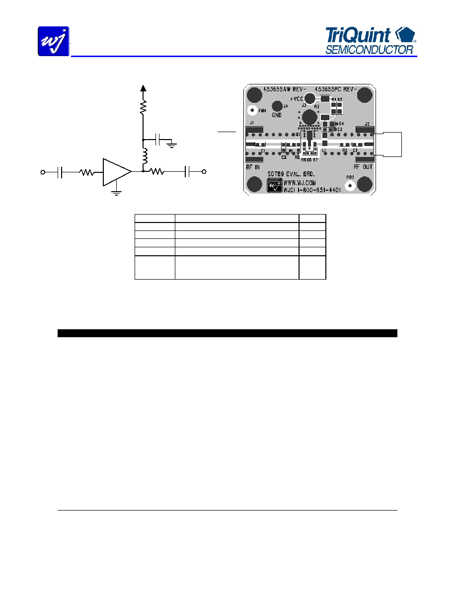
Application Circuit
Recommended Component Values
(1)
Ref. Name
Value / Type
Size
L1
470 nH ferrite core wire wound inductor (2)
0805
C1, C2
1000 pF NPO chip capacitor
0603
C3
0.018
μF chip capacitor
0603
R1, R2, R4
0
Ω(3)
0603
C4, C5, C6,
R3, R5, R6,
R7, R8
Do Not Place (3)
1.
The listed values are contained on the evaluation board to achieve optimal broadband performance
2.
For lower cost and performance (500 – 4000 MHz) option use 18 nH air core wire wound inductor.
3.
Place holders for the 0
Ω resistors and “Do Not Place” references are not needed for final design.
Typical Device Data
S-Parameters (Vdevice = +5 V, ICC = 80 mA, T = 25 °C, calibrated to device leads)
Freq (GHz)
S11 (dB)
S11 (ang)
S21 (dB)
S21 (ang)
S12 (dB)
S12 (ang)
S22 (dB)
S22 (ang)
10
-10.83
-58.08
19.46
164.89
-22.65
22.89
-7.78
-42.25
50
-12.23
-141.31
15.67
162.49
-19.17
8.66
-13.74
-117.02
100
-12.34
-161.16
14.97
166.07
-18.94
3.19
-15.40
-144.57
200
-12.35
-173.41
14.68
163.99
-18.79
-1.22
-16.18
-163.35
400
-12.20
178.57
14.70
155.01
-18.77
-6.50
-16.66
-176.66
600
-11.88
173.95
14.68
144.15
-18.79
-11.24
-16.93
174.89
800
-11.82
169.03
14.66
133.15
-18.73
-15.56
-17.11
171.49
1000
-11.96
160.89
14.73
122.08
-18.71
-19.47
-16.77
172.56
1200
-12.09
151.00
14.71
109.83
-18.72
-23.66
-16.57
175.62
1400
-12.00
141.47
14.72
98.56
-18.56
-28.45
-16.37
178.74
1600
-12.08
132.47
14.81
86.09
-18.56
-33.24
-16.52
179.44
1800
-12.41
124.96
14.89
73.48
-18.41
-37.07
-16.66
179.88
2000
-13.68
114.29
14.98
61.01
-18.32
-42.56
-16.10
-177.54
2200
-15.85
96.26
14.98
47.36
-18.25
-47.72
-14.74
-177.03
2400
-18.90
65.65
14.84
33.24
-18.25
-53.56
-12.91
-177.60
2600
-21.35
20.69
14.76
18.24
-18.22
-59.41
-11.52
-179.71
2800
-20.80
-41.45
14.49
3.96
-18.35
-66.15
-10.38
176.84
3000
-16.35
-85.03
14.02
-12.00
-18.44
-72.34
-9.38
170.50
3200
-12.38
-108.85
13.47
-27.18
-18.79
-78.26
-8.30
162.73
3400
-9.61
-124.63
12.65
-42.43
-19.07
-84.90
-7.42
153.42
3600
-7.75
-139.93
11.69
-56.65
-19.52
-89.74
-6.60
145.55
3800
-6.55
-155.31
10.76
-69.84
-19.79
-93.89
-6.01
140.59
4000
-5.60
-170.19
9.64
-82.81
-20.16
-98.32
-5.79
134.97
Device S-parameters are available for Download from the website at: http://www.wj.com
C1
Blocking
Capacitor
RF OUT
L1
RF Choke
C3
Bypass
Capacitor
R4
0
Ω
RF IN
C2
Blocking
Capacitor
Vcc = 5.00V
Icc = 80 mA
WJA1030
R1
0
Ω
R2
0
Ω
相关PDF资料 |
PDF描述 |
|---|---|
| WL600C/KG/GP1R | SPECIALTY TELECOM CIRCUIT |
| WL600C/KG/GP1R | SPECIALTY TELECOM CIRCUIT, PQFP48 |
| WMDE4M4V-80F1M | 4M X 4 EDO DRAM, 80 ns, CDSO24 |
| WMDE4M4V-80FPM | 4M X 4 EDO DRAM, 80 ns, CDFP24 |
| WMDE4M4V-100F1I | 4M X 4 EDO DRAM, 100 ns, CDSO24 |
相关代理商/技术参数 |
参数描述 |
|---|---|
| WJA1030-PCB | 功能描述:射频开发工具 50-2400MHz Eval Brd 15dB Gain RoHS:否 制造商:Taiyo Yuden 产品:Wireless Modules 类型:Wireless Audio 工具用于评估:WYSAAVDX7 频率: 工作电源电压:3.4 V to 5.5 V |
| WJA1030TR | 制造商:TriQuint Semiconductor 功能描述:GAIN BLOCK |
| WJA1035 | 功能描述:射频放大器 50-4000MHz +16dBm P1dB RoHS:否 制造商:Skyworks Solutions, Inc. 类型:Low Noise Amplifier 工作频率:2.3 GHz to 2.8 GHz P1dB:18.5 dBm 输出截获点:37.5 dBm 功率增益类型:32 dB 噪声系数:0.85 dB 工作电源电压:5 V 电源电流:125 mA 测试频率:2.6 GHz 最大工作温度:+ 85 C 安装风格:SMD/SMT 封装 / 箱体:QFN-16 封装:Reel |
| WJA1035-PCB | 功能描述:射频开发工具 50-2400MHz Eval Brd 15dB Gain RoHS:否 制造商:Taiyo Yuden 产品:Wireless Modules 类型:Wireless Audio 工具用于评估:WYSAAVDX7 频率: 工作电源电压:3.4 V to 5.5 V |
| WJA1035TR | 制造商:TriQuint Semiconductor 功能描述:GAIN BLOCK |
发布紧急采购,3分钟左右您将得到回复。