- 您现在的位置:买卖IC网 > PDF目录68583 > WJLXT388LEB2 (INTEL CORP) DATACOM, PCM TRANSCEIVER, PQFP100 PDF资料下载
参数资料
| 型号: | WJLXT388LEB2 |
| 厂商: | INTEL CORP |
| 元件分类: | 数字传输电路 |
| 英文描述: | DATACOM, PCM TRANSCEIVER, PQFP100 |
| 封装: | 14 X 14MM, ROHS COMPLIANT, LQFP-100 |
| 文件页数: | 9/80页 |
| 文件大小: | 1017K |
| 代理商: | WJLXT388LEB2 |
第1页第2页第3页第4页第5页第6页第7页第8页当前第9页第10页第11页第12页第13页第14页第15页第16页第17页第18页第19页第20页第21页第22页第23页第24页第25页第26页第27页第28页第29页第30页第31页第32页第33页第34页第35页第36页第37页第38页第39页第40页第41页第42页第43页第44页第45页第46页第47页第48页第49页第50页第51页第52页第53页第54页第55页第56页第57页第58页第59页第60页第61页第62页第63页第64页第65页第66页第67页第68页第69页第70页第71页第72页第73页第74页第75页第76页第77页第78页第79页第80页
Dual T1/E1/J1 Transceiver — Intel
LXT388
Datasheet
17
81
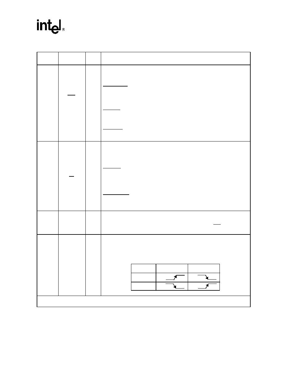
ACK/
RDY/
SDO
DO
Data Transfer acknowledge (Motorola Mode).
Ready (Intel mode).
Serial Data Output (Serial Mode).
Motorola Mode
A Low signal during a databus read operation indicates that the information is valid. A
Low signal during a write operation acknowledges that a data transfer into the addressed
register has been accepted (acknowledge signal).Wait states only occur if a write cycle
immediately follows a previous read or write cycle (e.g. read modify write).
Intel Mode
A High signal acknowledges that a register access operation has been completed (Ready
Signal). A Low signal on this pin signals that a data transfer operation is in progress. The
pin goes tristate after completion of a bus cycle.
Serial Mode
If CLKE is High, SDO is valid on the rising edge of SCLK. If CLKE is Low, SDO is valid on
the falling edge of SCLK. This pin goes into high Z state during a serial port write access.
82
ALE/
SCLK/
AS/
LEN2
DI
Address Latch Enable (Host Mode).
Shift Clock (Serial Mode).
Address Strobe (Motorola Mode).
Line Length Equalizer (Hardware Mode).
Host Mode
The address on the multiplexed address/data bus is clocked into the device with the
falling edge of ALE.
In serial Host mode this pin acts as serial shift clock.
In Motorola mode this pin acts a an active Low address strobe.
Hardware Mode
This pin determines the shape and amplitude of the transmit pulse in transceivers 0 and
1. It also determines the receiver setting (T1 or E1) in all the receivers. Please refer to
83
OE
DI
Output Driver Enable. If this pin is asserted Low all analog driver outputs immediately
enter a high impedance mode to support redundancy applications without external
mechanical relays. All other internal circuitry stays active. In software mode, TTIP and
TRING can be tristated on a port-by-port basis by writing a ‘1’ to the OEx bit in the Output
Enable Register (OER).
84
CLKE
DI
Clock Edge Select. In clock recovery mode, setting CLKE High causes RDATA or RPOS
and RNEG to be valid on the falling edge of RCLK and SDO to be valid on the rising edge
of SCLK. Setting CLKE Low makes RDATA or RPOS and RNEG to be valid on the rising
edge of RCLK and SDO to be valid on the falling edge of SCLK. In Data recovery Mode,
RDATA or RPOS/RNEG are active High output polarity when CLKE is High and active low
polarity when CLKE is Low.
Table 5.
Pin Assignments and Signal Descriptions - Microprocessor/Configuration
Pin #
LQFP
Symbol
I/O
1
Description
1. DI: Digital Input; DO: Digital Output; DI/O: Digital Bidirectional Port; AI: Analog Input; AO: Analog Output S: Power Supply;
N.C.: Not Connected.
CLKE
RPOS/RNEG
SDO
Low
High
SCLK
RCLK
相关PDF资料 |
PDF描述 |
|---|---|
| WJLXT388LEB2 | DATACOM, PCM TRANSCEIVER, PQFP100 |
| WJLXT901ALCA4 | DATACOM, ETHERNET TRANSCEIVER, PQFP64 |
| WJLXT907ALCA4 | DATACOM, ETHERNET TRANSCEIVER, PQFP64 |
| WJLXT901ALCA4 | DATACOM, ETHERNET TRANSCEIVER, PQFP64 |
| WJLXT907ALCA4 | DATACOM, ETHERNET TRANSCEIVER, PQFP64 |
相关代理商/技术参数 |
参数描述 |
|---|---|
| WJLXT6155LE.B5 | 制造商:Intel 功能描述:SONET/SDH/ATM Transceiver 1TX 1RX 64-Pin LQFP |
| WJLXT6155LE.B5-866255 | 功能描述:TXRX SDH/SONET/ATM HS 64-LQFP RoHS:是 类别:集成电路 (IC) >> 接口 - 驱动器,接收器,收发器 系列:- 产品培训模块:Lead (SnPb) Finish for COTS Obsolescence Mitigation Program 标准包装:50 系列:- 类型:收发器 驱动器/接收器数:1/1 规程:RS422,RS485 电源电压:4.75 V ~ 5.25 V 安装类型:通孔 封装/外壳:8-DIP(0.300",7.62mm) 供应商设备封装:8-PDIP 包装:管件 产品目录页面:1402 (CN2011-ZH PDF) |
| WJLXT6155LE.B5-866256 | 制造商:Cortina Systems Inc 功能描述:SONET/SDH/ATM Transceiver 1TX 1RX 64-Pin LQFP T/R |
| WJLXT901ALC.A4 | 功能描述:IC 10BASE-T/AUI TXCVR 64-LQFP RoHS:是 类别:集成电路 (IC) >> 接口 - 驱动器,接收器,收发器 系列:- 标准包装:1,000 系列:- 类型:收发器 驱动器/接收器数:2/2 规程:RS232 电源电压:3 V ~ 5.5 V 安装类型:表面贴装 封装/外壳:16-SOIC(0.295",7.50mm 宽) 供应商设备封装:16-SOIC 包装:带卷 (TR) |
| WJLXT901ALC.A4-865823 | 制造商:Cortina Systems Inc 功能描述:LXT901A UNIVERSAL ETHERNET TRA |
发布紧急采购,3分钟左右您将得到回复。