- 您现在的位置:买卖IC网 > PDF目录140439 > WMF512K8-90FEI5A 512K X 8 FLASH 5V PROM, 90 ns, CDFP32 PDF资料下载
参数资料
| 型号: | WMF512K8-90FEI5A |
| 元件分类: | PROM |
| 英文描述: | 512K X 8 FLASH 5V PROM, 90 ns, CDFP32 |
| 封装: | CERAMIC, FP-32 |
| 文件页数: | 6/13页 |
| 文件大小: | 156K |
| 代理商: | WMF512K8-90FEI5A |
2
White Electronic Designs Corporation Phoenix, AZ (602) 437-1520
WMF512K8-XXX5
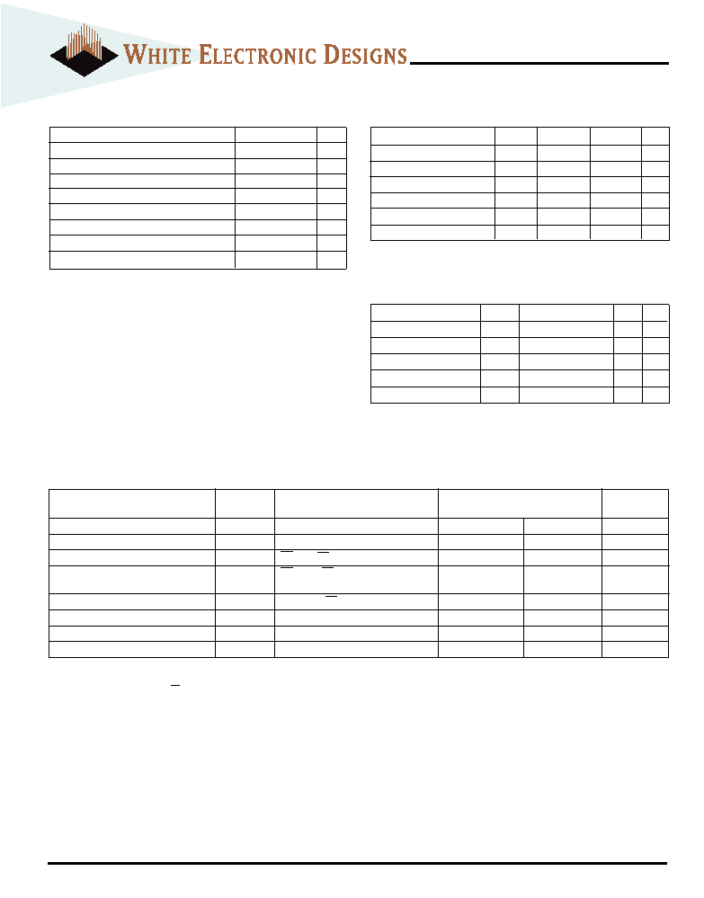
ABSOLUTE MAXIMUM RATINGS (1)
DC CHARACTERISTICS - CMOS COMPATIBLE
(VCC = 5.0V, VSS = 0V, TA = -55
°C to +125°C)
Parameter
Unit
Operating Temperature
-55 to +125
°C
Supply Voltage (VCC) (1)
-2.0 to +7.0
V
Signal Voltage Range(any pin except A9) (2)
-2.0 to +7.0
V
Storage Temperature Range
-65 to +150
°C
Lead Temperature (soldering, 10 seconds)
+300
°C
Data Retention Mil Temp
20
years
Endurance - erase/program cycles (Mil Temp)
100,000 min
cycles
A9 Voltage for sector protect (VID) (3)
-2.0 to +14.0
V
Parameter
Symbol
Conditions
Unit
Min
Max
Input Leakage Current
ILI
VCC = 5.5, VIN = GND to VCC
10
A
Output Leakage Current
ILOx32
VCC = 5.5, VIN = GND to VCC
10
A
VCC Active Current for Read (1)
ICC1
CS = VIL, OE = VIH, f = 5MHz
50
mA
VCC Active Current for Program
ICC2
CS = VIL, OE = VIH
or Erase (2)
60
mA
VCC Standby Current
ICC4
VCC = 5.5, CS = VIH, f = 5MHz
1.6
mA
Output Low Voltage
VOL
IOL = 8.0 mA, VCC = 4.5
0.45
V
Output High Voltage
VOH1
IOH = -2.5 mA, VCC = 4.5
0.85 x VCC
V
Low VCC Lock-Out Voltage
VLKO
3.2
4.2
V
RECOMMENDED OPERATING CONDITIONS
Parameter
Symbol
Min
Max
Unit
Supply Voltage
VCC
4.5
5.5
V
Input High Voltage
VIH
2.0
Vcc + 0.5
V
Input Low Voltage
VIL
-0.5
+0.8
V
Operating Temp. (Mil.)
TA
-55
+125
°C
Operating Temp. (Ind.)
TA
-40
+85
°C
A9 Voltage for Sector Protect
VID
11.5
12.5
V
NOTES:
1. Stresses above the absolute maximum rating may cause permanent damage
to the device. Extended operation at the maximum levels may degrade
performance and affect reliability.
2. Minimum DC voltage on input or I/O pins is -0.5V. During voltage transitions,
inputs may overshoot VSS to -2.0 V for periods of up to 20ns. Maximum DC
voltage on output and I/O pins is VCC + 0.5V. During voltage transitions,
outputs may overshoot to Vcc + 2.0 V for periods of up to 20ns.
3. Minimum DC input voltage on A9 pin is -0.5V. During voltage transitions, A9
may overshoot Vss to -2V for periods of up to 20ns. Maximum DC input
voltage on A9 is +13.5V which may overshoot to 14.0 V for periods up to 20ns.
CAPACITANCE
(TA = +25
°C)
Parameter
Symbol
Conditions
Max Unit
Address Input capacitance
CAD
VI/O = 0 V, f = 1.0 MHz
15
pF
Output Enable capacitance
COE
VIN = 0 V, f = 1.0 MHz
15
pF
Write Enable capacitance
CWE
VIN = 0 V, f = 1.0 MHz
15
pF
Chip Select capacitance
CCS
VIN = 0 V, f = 1.0 MHz
15
pF
Data I/O capacitance
CI/O
VI/O = 0 V, f = 1.0 MHz
15
pF
This parameter is guaranteed by design but not tested.
NOTES:
1. The ICC current listed includes both the DC operating current and the frequency dependent component (at 5 MHz). The frequency component typically
is less than 2 mA/MHz, with OE at VIH.
2. ICC active while Embedded Algorithm (program or erase) is in progress.
3. DC test conditions: VIL = 0.3V, VIH = VCC - 0.3V
相关PDF资料 |
PDF描述 |
|---|---|
| WMF512K8-120CC5A | 512K X 8 FLASH 5V PROM, 120 ns, CDIP32 |
| WMF512K8-90CM5 | 512K X 8 FLASH 5V PROM, 90 ns, CDIP32 |
| WMF512K8-70DEM5A | 512K X 8 FLASH 5V PROM, 70 ns, CDSO32 |
| WMF512K8-90DEC5 | 512K X 8 FLASH 5V PROM, 90 ns, CDSO32 |
| WMF512K8-120CLI5 | 512K X 8 FLASH 5V PROM, 120 ns, CQCC32 |
相关代理商/技术参数 |
参数描述 |
|---|---|
| WMF512K8-90FEM5 | 制造商:Microsemi Corporation 功能描述:512K X 8 FLASH MONOLITHIC, 5V, 90NS, 32 FLATPACK EVOL., MIL- - Bulk |
| WMF512K8-90FEM5A | 制造商:WEDC 制造商全称:White Electronic Designs Corporation 功能描述:512Kx8 MONOLITHIC FLASH, SMD 5962-96692 |
| WMF512K8-XCLX5 | 制造商:未知厂家 制造商全称:未知厂家 功能描述:Flash |
| WMF512K8-XCX5 | 制造商:未知厂家 制造商全称:未知厂家 功能描述:Flash |
| WMF512K8-XDEX5 | 制造商:未知厂家 制造商全称:未知厂家 功能描述:Flash |
发布紧急采购,3分钟左右您将得到回复。