- 您现在的位置:买卖IC网 > PDF目录245703 > WPS512K8LC-25RJIG (WHITE ELECTRONIC DESIGNS CORP) 512K X 8 STANDARD SRAM, 25 ns, PDSO36 PDF资料下载
参数资料
| 型号: | WPS512K8LC-25RJIG |
| 厂商: | WHITE ELECTRONIC DESIGNS CORP |
| 元件分类: | SRAM |
| 英文描述: | 512K X 8 STANDARD SRAM, 25 ns, PDSO36 |
| 封装: | ROHS COMPLIANT, PLASTIC, SOJ-36 |
| 文件页数: | 1/2页 |
| 文件大小: | 314K |
| 代理商: | WPS512K8LC-25RJIG |
1
White Electronic Designs Corporation (602) 437-1520 www.wedc.com
White Electronic Designs
EDI88512CA-XMXG
WPS512K8X-XRJXG
December 2008
Rev. 7
512Kx8 Plastic Monolithic SRAM CMOS
FEATURES
■
512Kx8 bit CMOS Static
■
Random Access Memory
Access Times of 17, 20, 25ns
Data Retention Function (LPA version)
Extended Temperature Testing
Data Retention Functionality Testing
■
36 lead JEDEC Approved Revolutionary Pinout
Plastic SOJ (Package 319)
■
Single +5V (±10%) Supply Operation
■
RoHS compliant
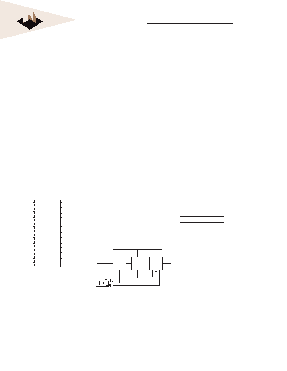
TOP VIEW
A0
A1
A2
A3
A4
CS#
I/O0
I/O1
VCC
VSS
I/O2
I/O3
WE#
A5
A6
A7
A8
A9
36pin
Revolutionary
NC
A18
A17
A16
A15
OE#
I/O7
I/O6
VSS
VCC
I/O5
I/O4
A14
A13
A12
A11
A10
NC
1
2
3
4
5
6
7
8
9
10
11
12
13
14
15
16
17
18
36
35
34
33
32
31
30
29
28
27
26
25
24
23
22
21
20
19
WEDC's ruggedized plastic 512Kx8 SRAM that allows
the user to capitalize on the cost advantage of using a
plastic component while not sacricing all of the reliability
available in a full military device.
Extended temperature testing is performed with the test
patterns developed for use on WEDC’s fully compliant
512Kx8 SRAMs. WEDC fully characterizes devices
to determine the proper test patterns for testing at
temperature extremes. This is critical because the
operating characteristics of device change when it is
operated beyond the commercial guarantee a device that
operates reliably in the eld at temperature extremes.
Users of WEDC’s ruggedized plastic benet from WEDC’s
extensive experience in characterizing SRAMs for use in
military systems.
WEDC ensures Low Power devices will retain data in Data
Retention mode by characterizing the devices to determine
the appropriate test conditions. This is crucial for systems
operating at -40°C or below and using dense memories
such as 512Kx8s.
WEDC’s ruggedized plastic SOJ is footprint compatible
with WEDC’s full military ceramic 36 pin SOJ.
PIN Description
I/O0-7
Data Inputs/Outputs
A0-18
Address Inputs
WE#
Write Enables
CS#
Chip Selects
OE#
Output Enable
VCC
Power (+5V ±10%)
VSS
Ground
NC
Not Connected
BLOCK DIAGRAM
WE#
CS#
OE#
Memory Array
Address
Buffer
Address
Decoder
I/O
Circuits
A-18
I/O-7
FIG. 1 – PIN CONFIGURATION
相关PDF资料 |
PDF描述 |
|---|---|
| WMS512K8M-45DEQ | 512K X 8 STANDARD SRAM, 45 ns, CDSO32 |
| WMF128K8-120FEI5 | 128K X 8 FLASH 5V PROM, 120 ns, CDFP32 |
| WMF128K8-70FEC5 | 128K X 8 FLASH 5V PROM, 70 ns, CDFP32 |
| WMF128K8-150CM5 | 128K X 8 FLASH 5V PROM, 150 ns, CDIP32 |
| WS57C51C-55J | 16K X 8 OTPROM, 55 ns, PQCC32 |
相关代理商/技术参数 |
参数描述 |
|---|---|
| WPS512K8LC-55TFM | 制造商:未知厂家 制造商全称:未知厂家 功能描述:x8 SRAM |
| WPS512K8LC-55TRM | 制造商:未知厂家 制造商全称:未知厂家 功能描述:x8 SRAM |
| WPS512K8LC-70TFM | 制造商:未知厂家 制造商全称:未知厂家 功能描述:x8 SRAM |
| WPS512K8LC-70TRM | 制造商:未知厂家 制造商全称:未知厂家 功能描述:x8 SRAM |
| WPS512K8LC-85TFM | 制造商:未知厂家 制造商全称:未知厂家 功能描述:x8 SRAM |
发布紧急采购,3分钟左右您将得到回复。