- 您现在的位置:买卖IC网 > PDF目录225548 > WV3HG128M72AER403D6MG (MICROSEMI CORP-PMG MICROELECTRONICS) 128M X 72 DDR DRAM MODULE, 0.6 ns, DMA240 PDF资料下载
参数资料
| 型号: | WV3HG128M72AER403D6MG |
| 厂商: | MICROSEMI CORP-PMG MICROELECTRONICS |
| 元件分类: | DRAM |
| 英文描述: | 128M X 72 DDR DRAM MODULE, 0.6 ns, DMA240 |
| 封装: | ROHS COMPLIANT, DIMM-240 |
| 文件页数: | 5/10页 |
| 文件大小: | 181K |
| 代理商: | WV3HG128M72AER403D6MG |
WV3HG128M72AER-D6
ADVANCED
4
White Electronic Designs Corporation (602) 437-1520 www.whiteedc.com
White Electronic Designs
October 2006
Rev. 1
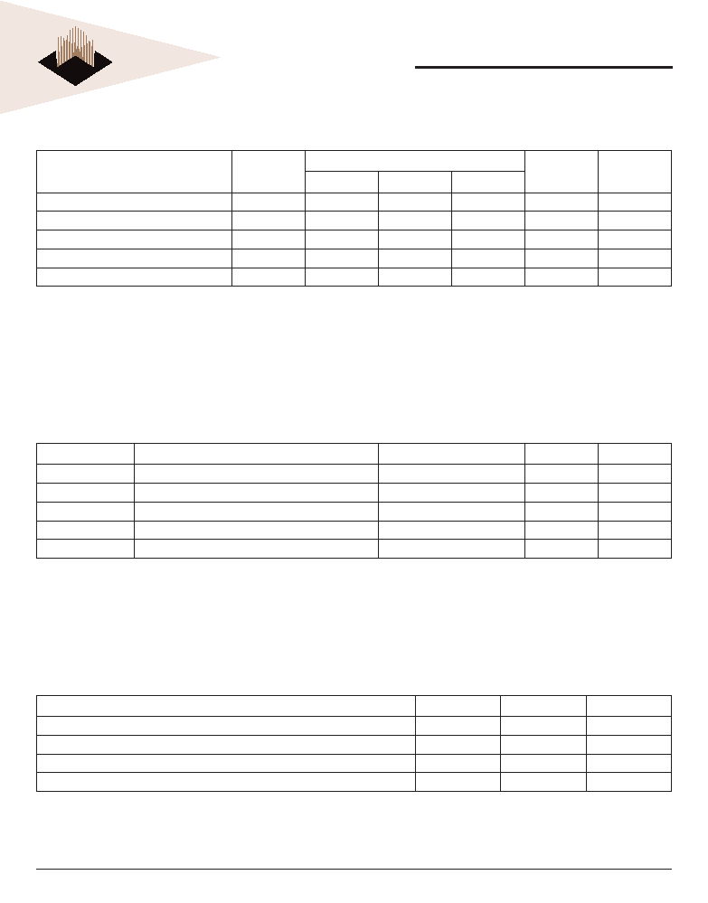
RECOMMENDED DC OPERATING CONDITIONS
All Voltages Referenced to VSS
Parameter
Symbol
Rating
Units
Notes
Min.
Type
Max.
Supply Voltage
VCC
1.7
1.8
1.9
V
Supply Voltage for DLL
VCCL
1.7
1.8
1.9
V
4
Supply Voltage for Output
VCCQ
1.7
1.8
1.9
V
4
Input Reference Voltage
VREF
0.49*VCCQ
0.50*VCCQ
0.51*VCCQ
V
1, 2
Termination Voltage
VTT
VREF-0.04
VREF
VREF+0.04
V
3
There is no specic device VCC supply voltage requirement for SSTL-1.8 compliance. However under all conditions VCCQ must be less than or equal to VCC.
1. The value of VREF may be selected by the user to provide optimum noise margin in the system. Typically the value of VREF is expected to be about 0.5 x VCCQ of the transmitting
device and VREF is expected to track variations in VCCQ.
2. Peak to peak AC noise on VREF may not exceed +/-2% VREF(DC).
3. VTT of transmitting device must track VREF of receiving device.
4. AC parameters are measured with VCC, VCCQ and VCCDL tied together.
ABSOLUTE MAXIMUM RATINGS
SSTL_1.8V
Symbol
Parameter
Rating
Units
Notes
VCC
Voltage on VCC pin relative to VSS
- 1.0 V - 2.3 V
V
5
VCCQ
Voltage on VCCQ pin relative to VSS
- 0.5 V - 2.3 V
V
5
VCCL
Voltage on VCCL pin relative to VSS
- 0.5 V - 2.3 V
V
5
VIN, VOUT
Voltage on any pin relative to VSS
- 0.5 V - 2.3 V
V
5
TSTG
Storage Temperature
-55 to +100
C
5, 6
5. Stresses greater than those listed under "Absolute Maximum Ratings" may cause permanent damage to the device. This is a stress rating only and functional operation of the
device at these or any other conditions above those indicated in the operational sections of this specication is not implied. Exposure to absolute maximum rating conditions for
extended periods may affect reliability.
6. Storage Temperature is the case surface temperature on the center/top side of the DRAM. For the measurement conditions, please refer to JESD51-2 standard.
CAPACITANCE
TA = 25°C, f = 1MHz, VCC = VCCQ = 1.8V
Parameter
Symbol
Max
Units
Input Capacitance: CK, CK#
CCK
11
pF
Input Capacitance: CKE, CS#
CI1
12
pF
Input Capacitance: Addr. RAS#, CAS#, WE#
CI2
12
pF
Input/Output Capacitance: DQ, DQS, DM, DQS#
CIO
10
pF
相关PDF资料 |
PDF描述 |
|---|---|
| WV3HG128M72AER534AD6MF | 128M X 72 DDR DRAM MODULE, 0.5 ns, DMA240 |
| WV3HG64M72AER403AD6SG | 64M X 72 DDR DRAM MODULE, 0.6 ns, DMA240 |
| WVL9EB681K | SHIELDED, VARIABLE INDUCTOR |
| WVLM0.15UH5% | SHIELDED, VARIABLE INDUCTOR |
| WVLM0.27UH5% | SHIELDED, VARIABLE INDUCTOR |
相关代理商/技术参数 |
参数描述 |
|---|---|
| WV3HG128M72AER403D6SG | 制造商:WEDC 制造商全称:White Electronic Designs Corporation 功能描述:1GB - 128Mx72 DDR2 SDRAM REGISTERED, w/PLL |
| WV3HG128M72AER534AD6EG | 制造商:WEDC 制造商全称:White Electronic Designs Corporation 功能描述:1GB - 128Mx72 DDR2 SDRAM RDIMM, VLP |
| WV3HG128M72AER534AD6IEG | 制造商:WEDC 制造商全称:White Electronic Designs Corporation 功能描述:1GB - 128Mx72 DDR2 SDRAM RDIMM, VLP |
| WV3HG128M72AER534AD6IMG | 制造商:WEDC 制造商全称:White Electronic Designs Corporation 功能描述:1GB - 128Mx72 DDR2 SDRAM RDIMM, VLP |
| WV3HG128M72AER534AD6ISG | 制造商:WEDC 制造商全称:White Electronic Designs Corporation 功能描述:1GB - 128Mx72 DDR2 SDRAM RDIMM, VLP |
发布紧急采购,3分钟左右您将得到回复。