参数资料
| 型号: | X1226V8IT2 |
| 厂商: | Intersil |
| 文件页数: | 25/25页 |
| 文件大小: | 0K |
| 描述: | IC RTC/CALENDAR/4K EE 8-TSSOP |
| 标准包装: | 2,500 |
| 类型: | 时钟/日历 |
| 特点: | 警报器,闰年 |
| 时间格式: | HH:MM:SS(12/24 小时) |
| 数据格式: | YY-MM-DD-dd |
| 接口: | I²C,2 线串口 |
| 电源电压: | 2.7 V ~ 5.5 V |
| 电压 - 电源,电池: | 1.8 V ~ 5.5 V |
| 工作温度: | -40°C ~ 85°C |
| 安装类型: | 表面贴装 |
| 封装/外壳: | 8-TSSOP(0.173",4.40mm 宽) |
| 供应商设备封装: | 8-TSSOP |
| 包装: | 带卷 (TR) |
9
FN8098.3
May 8, 2006
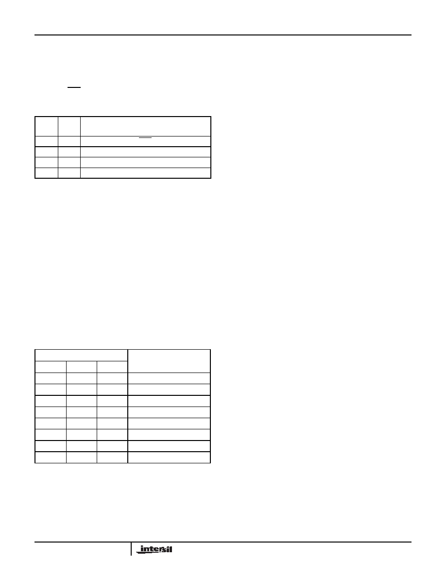
Programmable Frequency Output Bits—FO1, FO0
These are two output control bits. They select one of
three divisions of the internal oscillator, that is applied
to the PHZ output pin. Table 4 shows the selection bits
for this output. When using the PHZ output function,
the Alarm IRQ output function is disabled.
Table 4. Programmable Frequency Output Bits
ON-CHIP OSCILLATOR COMPENSATION
Digital Trimming Register (DTR) — DTR2, DTR1
and DTR0 (Non-Volatile)
The digital trimming Bits DTR2, DTR1 and DTR0
adjust the number of counts per second and average
the ppm error to achieve better accuracy.
DTR2 is a sign bit. DTR2 = 0 means frequency
compensation is > 0. DTR2 = 1 means frequency
compensation is < 0.
DTR1 and DTR0 are scale bits. DTR1 gives 10 ppm
adjustment and DTR0 gives 20 ppm adjustment.
A range from -30ppm to +30ppm can be represented
by using three bits above.
Table 5. Digital Trimming Registers
Analog Trimming Register (ATR) (Non-volatile)
Six analog trimming Bits from ATR5 to ATR0 are pro-
vided to adjust the on-chip loading capacitance range.
The on-chip load capacitance ranges from 3.25pF to
18.75pF. Each bit has a different weight for capaci-
tance adjustment. Using a Citizen CFS-206 crystal
with different ATR bit combinations provides an esti-
mated ppm range from +116ppm to -37ppm to the
nominal frequency compensation. The combination of
digital and analog trimming can give up to +146ppm
adjustment.
The on-chip capacitance can be calculated as follows:
CATR = [(ATR value, decimal) x 0.25pF] + 11.0pF
Note that the ATR values are in two’s complement,
with ATR(000000) = 11.0pF, so the entire range runs
from 3.25pF to 18.75pF in 0.25pF steps.
The values calculated above are typical, and total load
capacitance seen by the crystal will include approxi-
mately 2pF of package and board capacitance in addi-
tion to the ATR value.
See Application Section and Intersil’s Application Note
AN154 for more information.
WRITING TO THE CLOCK/CONTROL REGISTERS
Changing any of the nonvolatile bits of the
clock/control register requires the following steps:
– Write a 02h to the Status Register to set the Write
Enable Latch (WEL). This is a volatile operation, so
there is no delay after the write. (Operation pre-
ceeded by a start and ended with a stop).
– Write a 06h to the Status Register to set both the
Register Write Enable Latch (RWEL) and the WEL
bit. This is also a volatile cycle. The zeros in the data
byte are required. (Operation preceeded by a start
and ended with a stop).
– Write one to 8 bytes to the Clock/Control Registers
with the desired clock, alarm, or control data. This
sequence starts with a start bit, requires a slave byte
of “11011110” and an address within the CCR and is
terminated by a stop bit. A write to the CCR changes
EEPROM values so these initiate a nonvolatile write
cycle and will take up to 10ms to complete. Writes to
undefined areas have no effect. The RWEL bit is
reset by the completion of a nonvolatile write cycle,
so the sequence must be repeated to again initiate
another change to the CCR contents. If the
sequence is not completed for any reason (by send-
ing an incorrect number of bits or sending a start
instead of a stop, for example) the RWEL bit is not
reset and the device remains in an active mode.
– Writing all zeros to the status register resets both the
WEL and RWEL bits.
– A read operation occurring between any of the previ-
ous operations will not interrupt the register write
operation.
FO1
FO0
Output Frequency
(average of 100 samples)
00
Alarm IRQ output
0
1
32.768kHz
1
0
4096Hz
11
1Hz
DTR Register
Estimated frequency
PPM
DTR2
DTR1
DTR0
00
0
01
0
+10
00
1
+20
01
1
+30
10
0
11
0
-10
10
1
-20
11
1
-30
X1226
相关PDF资料 |
PDF描述 |
|---|---|
| MS27473E22A1PA | CONN PLUG 100POS STRAIGHT W/PINS |
| VE-BNH-MY-F4 | CONVERTER MOD DC/DC 52V 50W |
| MS27656T21B35SC | CONN RCPT 79POS WALL MNT W/SCKT |
| X1226S8T2 | IC RTC/CALENDAR/4K EE 8-SOIC |
| VE-BNH-MY-F3 | CONVERTER MOD DC/DC 52V 50W |
相关代理商/技术参数 |
参数描述 |
|---|---|
| X1226V8IZ | 功能描述:IC RTC/CALENDAR/ALARM 4K 8-TSSOP RoHS:是 类别:集成电路 (IC) >> 时钟/计时 - 实时时钟 系列:- 产品培训模块:Obsolescence Mitigation Program 标准包装:1 系列:- 类型:时钟/日历 特点:警报器,闰年,SRAM 存储容量:- 时间格式:HH:MM:SS(12/24 小时) 数据格式:YY-MM-DD-dd 接口:SPI 电源电压:2 V ~ 5.5 V 电压 - 电源,电池:- 工作温度:-40°C ~ 85°C 安装类型:表面贴装 封装/外壳:8-WDFN 裸露焊盘 供应商设备封装:8-TDFN EP 包装:管件 |
| X1226V8IZT1 | 功能描述:IC RTC/CALENDAR/ALARM 4K 8-TSSOP RoHS:是 类别:集成电路 (IC) >> 时钟/计时 - 实时时钟 系列:- 产品培训模块:Obsolescence Mitigation Program 标准包装:1 系列:- 类型:时钟/日历 特点:警报器,闰年,SRAM 存储容量:- 时间格式:HH:MM:SS(12/24 小时) 数据格式:YY-MM-DD-dd 接口:SPI 电源电压:2 V ~ 5.5 V 电压 - 电源,电池:- 工作温度:-40°C ~ 85°C 安装类型:表面贴装 封装/外壳:8-WDFN 裸露焊盘 供应商设备封装:8-TDFN EP 包装:管件 |
| X1226V8T1 | 功能描述:IC RTC/CALENDAR/4K EE 8-TSSOP RoHS:否 类别:集成电路 (IC) >> 时钟/计时 - 实时时钟 系列:- 产品培训模块:Obsolescence Mitigation Program 标准包装:1 系列:- 类型:时钟/日历 特点:警报器,闰年,SRAM 存储容量:- 时间格式:HH:MM:SS(12/24 小时) 数据格式:YY-MM-DD-dd 接口:SPI 电源电压:2 V ~ 5.5 V 电压 - 电源,电池:- 工作温度:-40°C ~ 85°C 安装类型:表面贴装 封装/外壳:8-WDFN 裸露焊盘 供应商设备封装:8-TDFN EP 包装:管件 |
| X1226V8T2 | 功能描述:IC RTC/CALENDAR/4K EE 8-TSSOP RoHS:否 类别:集成电路 (IC) >> 时钟/计时 - 实时时钟 系列:- 产品培训模块:Obsolescence Mitigation Program 标准包装:1 系列:- 类型:时钟/日历 特点:警报器,闰年,SRAM 存储容量:- 时间格式:HH:MM:SS(12/24 小时) 数据格式:YY-MM-DD-dd 接口:SPI 电源电压:2 V ~ 5.5 V 电压 - 电源,电池:- 工作温度:-40°C ~ 85°C 安装类型:表面贴装 封装/外壳:8-WDFN 裸露焊盘 供应商设备封装:8-TDFN EP 包装:管件 |
| X1226V8Z | 功能描述:IC RTC/CALENDAR/4K EE 8-TSSOP RoHS:是 类别:集成电路 (IC) >> 时钟/计时 - 实时时钟 系列:- 产品培训模块:Obsolescence Mitigation Program 标准包装:1 系列:- 类型:时钟/日历 特点:警报器,闰年,SRAM 存储容量:- 时间格式:HH:MM:SS(12/24 小时) 数据格式:YY-MM-DD-dd 接口:SPI 电源电压:2 V ~ 5.5 V 电压 - 电源,电池:- 工作温度:-40°C ~ 85°C 安装类型:表面贴装 封装/外壳:8-WDFN 裸露焊盘 供应商设备封装:8-TDFN EP 包装:管件 |
发布紧急采购,3分钟左右您将得到回复。