参数资料
| 型号: | X1227S8Z-2.7A |
| 厂商: | Intersil |
| 文件页数: | 10/28页 |
| 文件大小: | 0K |
| 描述: | IC RTC/CAL/CPU SUP EE 8-SOIC |
| 标准包装: | 100 |
| 类型: | 时钟/日历 |
| 特点: | 警报器,闰年,监控器,监视计时器 |
| 时间格式: | HH:MM:SS(12/24 小时) |
| 数据格式: | YY-MM-DD-dd |
| 接口: | I²C,2 线串口 |
| 电源电压: | 2.7 V ~ 5.5 V |
| 电压 - 电源,电池: | 1.8 V ~ 5.5 V |
| 工作温度: | 0°C ~ 70°C |
| 安装类型: | 表面贴装 |
| 封装/外壳: | 8-SOIC(0.154",3.90mm 宽) |
| 供应商设备封装: | 8-SOIC |
| 包装: | 管件 |
第1页第2页第3页第4页第5页第6页第7页第8页第9页当前第10页第11页第12页第13页第14页第15页第16页第17页第18页第19页第20页第21页第22页第23页第24页第25页第26页第27页第28页
18
FN8099.2
May 8, 2006
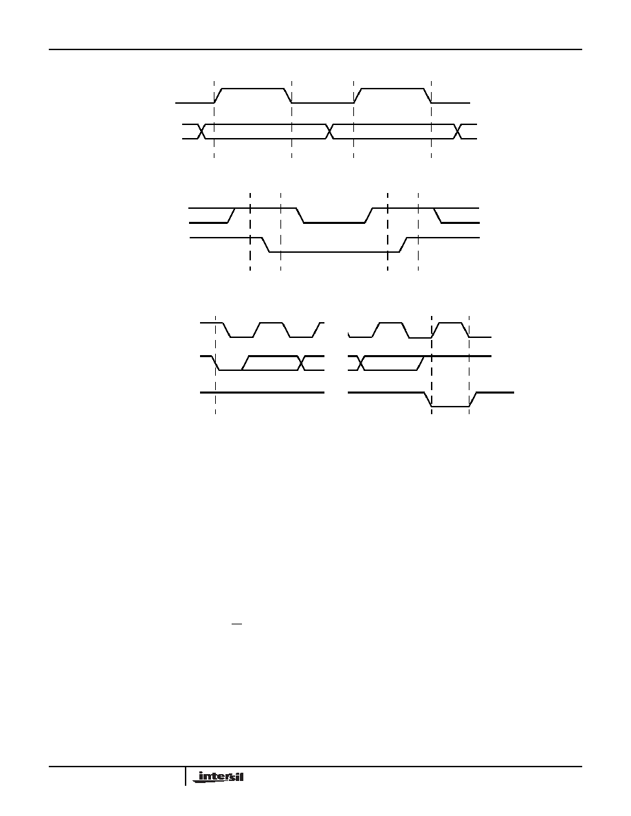
Figure 8. Valid Data Changes on the SDA Bus
Figure 9. Valid Start and Stop Conditions
Figure 10. Acknowledge Response From Receiver
DEVICE ADDRESSING
Following a start condition, the master must output a
Slave Address Byte. The first four bits of the Slave
Address Byte specify access to either the EEPROM
array or to the CCR. Slave bits ‘1010’ access the
EEPROM array. Slave bits ‘1101’ access the CCR.
When shipped from the factory, EEPROM array is
UNDEFINED, and should be programmed by the cus-
tomer to a known state.
Bit 3 through Bit 1 of the slave byte specify the device
select bits. These are set to ‘111’.
The last bit of the Slave Address Byte defines the
operation to be performed. When this R/W bit is a one,
then a read operation is selected. A zero selects a
write operation. Refer to Figure 11.
After loading the entire Slave Address Byte from the
SDA bus, the X1227 compares the device identifier
and device select bits with ‘1010111’ or ‘1101111’.
Upon a correct compare, the device outputs an
acknowledge on the SDA line.
Following the Slave Byte is a two byte word address.
The word address is either supplied by the master
device or obtained from an internal counter. On power-
up the internal address counter is set to address 0h,
so a current address read of the EEPROM array starts
at address 0. When required, as part of a random
read, the master must supply the 2 Word Address
Bytes as shown in Figure 11.
In a random read operation, the slave byte in the
“dummy write” portion must match the slave byte in
the “read” section. That is if the random read is from
the array the slave byte must be 1010111x in both
instances. Similarly, for a random read of the
Clock/Control Registers, the slave byte must be
1101111x in both places.
SCL
SDA
Data Stable
Data Change
Data Stable
SCL
SDA
Start
Stop
SCL from
Master
Data Output
from Transmitter
Data Output
from Receiver
8
1
9
Start
Acknowledge
X1227
相关PDF资料 |
PDF描述 |
|---|---|
| X1227S8Z-2.7 | IC RTC/CAL/CPU SUP EE 8-SOIC |
| MCP4251T-103E/ML | IC DGTL POT 10K 2CH 16QFN |
| X1227S8Z | IC RTC/CAL/CPU SUP EE 8-SOIC |
| MCP4251T-103E/SL | IC DGTL POT 10K 2CH 14SOIC |
| X1227S8T1 | IC RTC/CAL/CPU SUP EE 8-SOIC |
相关代理商/技术参数 |
参数描述 |
|---|---|
| X1227S8Z-4.5A | 功能描述:IC RTC/CAL/CPU SUP EE 8-SOIC RoHS:是 类别:集成电路 (IC) >> 时钟/计时 - 实时时钟 系列:- 产品培训模块:Obsolescence Mitigation Program 标准包装:1 系列:- 类型:时钟/日历 特点:警报器,闰年,SRAM 存储容量:- 时间格式:HH:MM:SS(12/24 小时) 数据格式:YY-MM-DD-dd 接口:SPI 电源电压:2 V ~ 5.5 V 电压 - 电源,电池:- 工作温度:-40°C ~ 85°C 安装类型:表面贴装 封装/外壳:8-WDFN 裸露焊盘 供应商设备封装:8-TDFN EP 包装:管件 |
| X1227S8ZT1 | 功能描述:IC RTC/CAL/CPU SUP EE 8-SOIC RoHS:是 类别:集成电路 (IC) >> 时钟/计时 - 实时时钟 系列:- 产品培训模块:Obsolescence Mitigation Program 标准包装:1 系列:- 类型:时钟/日历 特点:警报器,闰年,SRAM 存储容量:- 时间格式:HH:MM:SS(12/24 小时) 数据格式:YY-MM-DD-dd 接口:SPI 电源电压:2 V ~ 5.5 V 电压 - 电源,电池:- 工作温度:-40°C ~ 85°C 安装类型:表面贴装 封装/外壳:8-WDFN 裸露焊盘 供应商设备封装:8-TDFN EP 包装:管件 |
| X1227V8 | 功能描述:IC RTC/CAL/CPU SUP EE 8-TSSOP RoHS:否 类别:集成电路 (IC) >> 时钟/计时 - 实时时钟 系列:- 产品培训模块:Obsolescence Mitigation Program 标准包装:1 系列:- 类型:时钟/日历 特点:警报器,闰年,SRAM 存储容量:- 时间格式:HH:MM:SS(12/24 小时) 数据格式:YY-MM-DD-dd 接口:SPI 电源电压:2 V ~ 5.5 V 电压 - 电源,电池:- 工作温度:-40°C ~ 85°C 安装类型:表面贴装 封装/外壳:8-WDFN 裸露焊盘 供应商设备封装:8-TDFN EP 包装:管件 |
| X1227V8-2.7 | 功能描述:IC RTC/CAL/CPU SUP EE 8-TSSOP RoHS:否 类别:集成电路 (IC) >> 时钟/计时 - 实时时钟 系列:- 产品培训模块:Obsolescence Mitigation Program 标准包装:1 系列:- 类型:时钟/日历 特点:警报器,闰年,SRAM 存储容量:- 时间格式:HH:MM:SS(12/24 小时) 数据格式:YY-MM-DD-dd 接口:SPI 电源电压:2 V ~ 5.5 V 电压 - 电源,电池:- 工作温度:-40°C ~ 85°C 安装类型:表面贴装 封装/外壳:8-WDFN 裸露焊盘 供应商设备封装:8-TDFN EP 包装:管件 |
| X1227V8-2.7A | 功能描述:IC RTC/CAL/CPU SUP EE 8-TSSOP RoHS:否 类别:集成电路 (IC) >> 时钟/计时 - 实时时钟 系列:- 产品培训模块:Obsolescence Mitigation Program 标准包装:1 系列:- 类型:时钟/日历 特点:警报器,闰年,SRAM 存储容量:- 时间格式:HH:MM:SS(12/24 小时) 数据格式:YY-MM-DD-dd 接口:SPI 电源电压:2 V ~ 5.5 V 电压 - 电源,电池:- 工作温度:-40°C ~ 85°C 安装类型:表面贴装 封装/外壳:8-WDFN 裸露焊盘 供应商设备封装:8-TDFN EP 包装:管件 |
发布紧急采购,3分钟左右您将得到回复。