参数资料
| 型号: | X1286A8 |
| 厂商: | Intersil |
| 文件页数: | 8/25页 |
| 文件大小: | 0K |
| 描述: | IC RTC/CAL/CPU SUP EE 8EIAJSOIC |
| 标准包装: | 94 |
| 类型: | 时钟/日历 |
| 特点: | 警报器,闰年,监控器,监视计时器 |
| 时间格式: | HH:MM:SS:hh(12/24 小时) |
| 数据格式: | YY-MM-DD-dd |
| 接口: | I²C,2 线串口 |
| 电源电压: | 2.7 V ~ 5.5 V |
| 电压 - 电源,电池: | 1.8 V ~ 5.5 V |
| 工作温度: | 0°C ~ 70°C |
| 安装类型: | 表面贴装 |
| 封装/外壳: | 8-SOIC(0.209",5.30mm 宽) |
| 供应商设备封装: | 8-SOIC |
| 包装: | 管件 |
16
FN8101.1
April 14, 2006
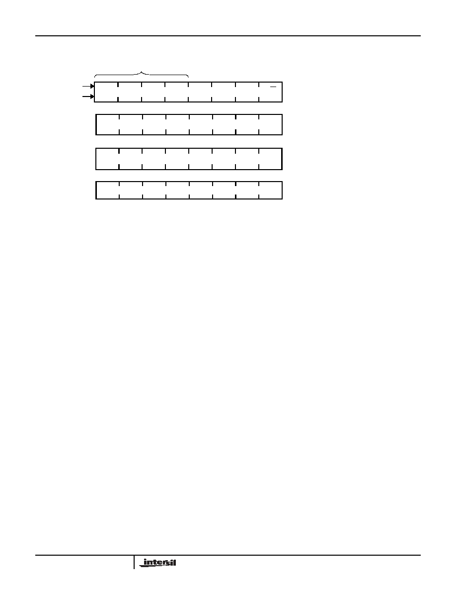
Figure 7. Slave Address, Word Address, and Data Bytes (128 Byte pages)
Write Operations
Byte Write
For a write operation, the device requires the Slave
Address Byte and the Word Address Bytes. This gives
the master access to any one of the words in the array
or CCR. (Note: Prior to writing to the CCR, the master
must write a 02h, then 06h to the status register in two
preceding operations to enable the write operation.
See “Writing to the Clock/Control Registers.” Upon
receipt of each address byte, the X1286 responds with
an acknowledge. After receiving both address bytes
the X1286 awaits the eight bits of data. After receiving
the 8 data bits, the X1286 again responds with an
acknowledge. The master then terminates the transfer
by generating a stop condition. The X1286 then
begins an internal write cycle of the data to the nonvol-
atile memory. During the internal write cycle, the
device inputs are disabled, so the device will not
respond to any requests from the master. The SDA out-
put is at high impedance. See Figure 8.
A write to a protected block of memory is ignored, but
will still receive an acknowledge. At the end of the
write command, the X1286 will not initiate an internal
write cycle, and will continue to ACK commands.
Page Write
The X1286 has a page write operation. It is initiated in
the same manner as the byte write operation; but
instead of terminating the write cycle after the first data
byte is transferred, the master can transmit up to 127
more bytes to the memory array and up to 7 more
bytes to the clock/control registers. (Note: Prior to writ-
ing to the CCR, the master must write a 02h, then 06h
to the status register in two preceding operations to
enable the write operation. See “Writing to the
Clock/Control Registers.”
After the receipt of each byte, the X1286 responds
with an acknowledge, and the address is internally
incremented by one. When the counter reaches the
end of the page, it “rolls over” and goes back to the
first address on the same page. This means that the
master can write 128 bytes to a memory array page or
8 bytes to a CCR section starting at any location on
that page. For example, if the master begins writing at
location 105 of the memory and loads 30 bytes, then
the first 23 bytes are written to addresses 105 through
127, and the last 7 bytes are written to columns 0
through 6. Afterwards, the address counter would
point to location 7 on the page that was just written. If
the master supplies more than the maximum bytes in
a page, then the previously loaded data is over written
by the new data, one byte at a time. Refer to Figure 9.
The master terminates the Data Byte loading by issu-
ing a stop condition, which causes the X1286 to begin
the nonvolatile write cycle. As with the byte write oper-
ation, all inputs are disabled until completion of the
internal write cycle. Refer to Figure 10 for the address,
acknowledge, and data transfer sequence.
Stops and Write Modes
Stop conditions that terminate write operations must
be sent by the master after sending at least 1 full data
byte and it’s associated ACK signal. If a stop is issued
in the middle of a data byte, or before 1 full data byte +
ACK is sent, then the X1286 resets itself without per-
forming the write. The contents of the array are not
affected.
Slave Address Byte
Byte 0
D7
D6
D5
D2
D4
D3
D1
D0
A0
A7
A2
A4
A3
A1
Data Byte
Byte 3
A6
A5
0
A14
A11
A10
A9
A8
A12
1
0
1
0
1
0
1
R/W
1
Device Identifier
Array
CCR
A13
Word Address 1
Byte 1
Word Address 0
Byte 2
X1286
相关PDF资料 |
PDF描述 |
|---|---|
| X1288V14Z-4.5AT1 | IC RTC/CAL/CPU SUP EE 14-TSSOP |
| X1288V14Z-2.7AT1 | IC RTC/CAL/CPU SUP EE 14-TSSOP |
| X1288V14Z-2.7T1 | IC RTC/CAL/CPU SUP EE 14-TSSOP |
| X1288V14Z-4.5A | IC RTC/CAL/CPU SUP EE 14-TSSOP |
| X1288V14Z-2.7 | IC RTC/CAL/CPU SUP EE 14-TSSOP |
相关代理商/技术参数 |
参数描述 |
|---|---|
| X1286A8I | 制造商:INTERSIL 制造商全称:Intersil Corporation 功能描述:Intersil Real Time Clock/Calendar/CPU Supervisor with EEPROM X1286 |
| X1286A8IT1 | 功能描述:IC RTC/CAL/CPU SUP EE 8EIAJSOIC RoHS:否 类别:集成电路 (IC) >> 时钟/计时 - 实时时钟 系列:- 产品培训模块:Obsolescence Mitigation Program 标准包装:1 系列:- 类型:时钟/日历 特点:警报器,闰年,SRAM 存储容量:- 时间格式:HH:MM:SS(12/24 小时) 数据格式:YY-MM-DD-dd 接口:SPI 电源电压:2 V ~ 5.5 V 电压 - 电源,电池:- 工作温度:-40°C ~ 85°C 安装类型:表面贴装 封装/外壳:8-WDFN 裸露焊盘 供应商设备封装:8-TDFN EP 包装:管件 |
| X1286A8T1 | 功能描述:IC RTC/CAL/CPU SUP EE 8EIAJSOIC RoHS:否 类别:集成电路 (IC) >> 时钟/计时 - 实时时钟 系列:- 产品培训模块:Obsolescence Mitigation Program 标准包装:1 系列:- 类型:时钟/日历 特点:警报器,闰年,SRAM 存储容量:- 时间格式:HH:MM:SS(12/24 小时) 数据格式:YY-MM-DD-dd 接口:SPI 电源电压:2 V ~ 5.5 V 电压 - 电源,电池:- 工作温度:-40°C ~ 85°C 安装类型:表面贴装 封装/外壳:8-WDFN 裸露焊盘 供应商设备封装:8-TDFN EP 包装:管件 |
| X1286V14 | 功能描述:IC RTC/CAL/CPU SUP EE 14-TSSOP RoHS:否 类别:集成电路 (IC) >> 时钟/计时 - 实时时钟 系列:- 产品培训模块:Obsolescence Mitigation Program 标准包装:1 系列:- 类型:时钟/日历 特点:警报器,闰年,SRAM 存储容量:- 时间格式:HH:MM:SS(12/24 小时) 数据格式:YY-MM-DD-dd 接口:SPI 电源电压:2 V ~ 5.5 V 电压 - 电源,电池:- 工作温度:-40°C ~ 85°C 安装类型:表面贴装 封装/外壳:8-WDFN 裸露焊盘 供应商设备封装:8-TDFN EP 包装:管件 |
| X1286V14I | 功能描述:IC RTC/CAL/CPU SUP EE 14-TSSOP RoHS:否 类别:集成电路 (IC) >> 时钟/计时 - 实时时钟 系列:- 产品培训模块:Obsolescence Mitigation Program 标准包装:1 系列:- 类型:时钟/日历 特点:警报器,闰年,SRAM 存储容量:- 时间格式:HH:MM:SS(12/24 小时) 数据格式:YY-MM-DD-dd 接口:SPI 电源电压:2 V ~ 5.5 V 电压 - 电源,电池:- 工作温度:-40°C ~ 85°C 安装类型:表面贴装 封装/外壳:8-WDFN 裸露焊盘 供应商设备封装:8-TDFN EP 包装:管件 |
发布紧急采购,3分钟左右您将得到回复。