- 您现在的位置:买卖IC网 > PDF目录15102 > X5001S8Z-2.7 (Intersil)IC SUPERVISOR CPU 8-SOIC PDF资料下载
参数资料
| 型号: | X5001S8Z-2.7 |
| 厂商: | Intersil |
| 文件页数: | 4/20页 |
| 文件大小: | 0K |
| 描述: | IC SUPERVISOR CPU 8-SOIC |
| 标准包装: | 100 |
| 类型: | 简单复位/加电复位 |
| 监视电压数目: | 1 |
| 输出: | 开路漏极或开路集电极 |
| 复位: | 低有效 |
| 复位超时: | 最小为 100 ms |
| 电压 - 阀值: | 2.63V |
| 工作温度: | 0°C ~ 70°C |
| 安装类型: | 表面贴装 |
| 封装/外壳: | 8-SOIC(0.154",3.90mm 宽) |
| 供应商设备封装: | 8-SO |
| 包装: | 管件 |
�� �
�
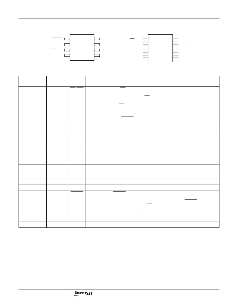
�X5001�
�PIN� CONFIGURATION�
�8� Ld� TSSOP�
�8� Ld� SOIC/PDIP�
�RESET�
�1�
�8�
�SCK�
�CS/WDI�
�1�
�8�
�V� CC�
�V� CC�
�CS/WDI�
�SO�
�2�
�3�
�4�
�X5001�
�7�
�6�
�5�
�SI�
�V� SS�
�V� PE�
�SO�
�V� PE�
�V� SS�
�2�
�3�
�4�
�X5001�
�7�
�6�
�5�
�RESET�
�SCK�
�SI�
�PIN� DESCRIPTION�
�Pin�
�(SOIC/PDIP)�
�1�
�Pin�
�TSSOP�
�1�
�Name�
�CS/WDI�
�Function�
�Chip� Select� Input.� CS� HIGH,� deselects� the� device� and� the� SO� output� pin� is� at�
�a� high� impedance� state.� Unless� a� nonvolatile� write� cycle� is� underway,� the� device�
�will� be� in� the� standby� power� mode.� CS� LOW� enables� the� device,� placing� it� in� the�
�active� power� mode.� Prior� to� the� start� of� any� operation� after� power-up,� a� HIGH� to�
�LOW� transition� on� CS� is� required.�
�Watchdog� Input.� A� HIGH� to� LOW� transition� on� the� WDI� pin� restarts� the� Watch-�
�dog� timer.� The� absence� of� a� HIGH� to� LOW� transition� within� the� watchdog� time�
�out� period� results� in� RESET/RESET� going� active.�
�2�
�5�
�6�
�3�
�4�
�8�
�7�
�2�
�8�
�9�
�6�
�7�
�14�
�13�
�3-5,10-12�
�4�
�SO�
�SI�
�SCK�
�V� PE�
�V� SS�
�V� CC�
�RESET�
�NC�
�Serial� Output.� SO� is� a� push/pull� serial� data� output� pin.� A� read� cycle� shifts� data�
�out� on� this� pin.� The� falling� edge� of� the� serial� clock� (SCK)� clocks� the� data� out.�
�Serial� Input.� SI� is� a� serial� data� input� pin.� Input� all� opcodes,� byte� addresses,� and�
�memory� data� on� this� pin.� The� rising� edge� of� the� serial� clock� (SCK)� latches� the�
�input� data.� Send� all� opcodes� (Table� 1),� addresses� and� data� MSB� first.�
�Serial� Clock.� The� Serial� Clock� controls� the� serial� bus� timing� for� data� input� and�
�output.� The� rising� edge� of� SCK� latches� in� the� opcode,� address,� or� watchdog� bits�
�present� on� the� SI� pin.� The� falling� edge� of� SCK� changes� the� data� output� on� the�
�SO� pin.�
�V� TRIP� Program� Enable.� When� V� PE� is� LOW,� the� V� TRIP� point� is� fixed� at� the� last�
�valid� programmed� level.� To� readjust� the� V� TRIP� level,� requires� that� the� V� PE� pin� be�
�pulled� to� a� high� voltage� (15-18V).�
�Ground�
�Supply� Voltage�
�Reset� Output� .� RESET� is� an� active� LOW,� open� drain� output� which� goes� active�
�whenever� V� CC� falls� below� the� minimum� V� CC� sense� level.� It� will� remain� active� un-�
�til� V� CC� rises� above� the� minimum� V� CC� sense� level� for� 200ms.� RESET� goes� active�
�if� the� watchdog� timer� is� enabled� and� CS/WDI� remains� either� HIGH� or� LOW� long-�
�er� than� the� selectable� watchdog� time� out� period.� A� falling� edge� of� CS/WDI� will�
�reset� the� watchdog� timer.� RESET� goes� active� on� power-up� at� 1V� and� remains�
�active� for� 200ms� after� the� power� supply� stabilizes.�
�No� internal� connections�
�FN8125.1�
�May� 30,� 2006�
�相关PDF资料 |
PDF描述 |
|---|---|
| ACM11DSEN-S13 | CONN EDGECARD EXTEND 22POS 0.156 |
| VE-B1Z-EU-F4 | CONVERTER MOD DC/DC 2V 80W |
| LT3845MPFE#TR | IC REG CTRLR BUCK PWM CM 16TSSOP |
| B43088A2107M | 100UF 200V 16X25 SINGLE END |
| SN222M010ST | CAP ALUM 2200UF 10V 20% RADIAL |
相关代理商/技术参数 |
参数描述 |
|---|---|
| X5001S8Z-4.5A | 功能描述:IC SUPERVISOR CPU 8-SOIC RoHS:是 类别:集成电路 (IC) >> PMIC - 监控器 系列:- 产品培训模块:Lead (SnPb) Finish for COTS Obsolescence Mitigation Program 标准包装:2,500 系列:- 类型:简单复位/加电复位 监视电压数目:1 输出:开路漏极或开路集电极 复位:低有效 复位超时:最小为 600 ms 电压 - 阀值:3.8V 工作温度:-40°C ~ 85°C 安装类型:表面贴装 封装/外壳:SC-74A,SOT-753 供应商设备封装:SOT-23-5 包装:带卷 (TR) |
| X5001V8 | 功能描述:IC SUPERVISOR CPU 8-TSSOP RoHS:否 类别:集成电路 (IC) >> PMIC - 监控器 系列:- 标准包装:100 系列:- 类型:简单复位/加电复位 监视电压数目:1 输出:- 复位:低有效 复位超时:最小为 100 ms 电压 - 阀值:4.38V 工作温度:0°C ~ 70°C 安装类型:表面贴装 封装/外壳:8-TSSOP(0.173",4.40mm 宽) 供应商设备封装:8-TSSOP 包装:管件 |
| X5001V8-1.8 | 制造商:未知厂家 制造商全称:未知厂家 功能描述:Power Supply Supervisor |
| X5001V8-2.7 | 功能描述:IC SUPERVISOR CPU 8-TSSOP RoHS:否 类别:集成电路 (IC) >> PMIC - 监控器 系列:- 产品培训模块:Lead (SnPb) Finish for COTS Obsolescence Mitigation Program 标准包装:2,500 系列:- 类型:简单复位/加电复位 监视电压数目:1 输出:推挽式,图腾柱 复位:低有效 复位超时:最小 145 ms 电压 - 阀值:2.64V 工作温度:-40°C ~ 85°C 安装类型:表面贴装 封装/外壳:16-WQFN 裸露焊盘 供应商设备封装:16-TQFN-EP(4x4) 包装:带卷 (TR) |
| X5001V8-2.7A | 功能描述:IC SUPERVISOR CPU 8-TSSOP RoHS:否 类别:集成电路 (IC) >> PMIC - 监控器 系列:- 产品培训模块:Lead (SnPb) Finish for COTS Obsolescence Mitigation Program 标准包装:2,500 系列:- 类型:简单复位/加电复位 监视电压数目:1 输出:推挽式,图腾柱 复位:低有效 复位超时:最小 145 ms 电压 - 阀值:2.64V 工作温度:-40°C ~ 85°C 安装类型:表面贴装 封装/外壳:16-WQFN 裸露焊盘 供应商设备封装:16-TQFN-EP(4x4) 包装:带卷 (TR) |
发布紧急采购,3分钟左右您将得到回复。