- 您现在的位置:买卖IC网 > PDF目录10775 > X79001V20I (Intersil)IC DAC NV SELECT OUT/MEM 20TSSOP PDF资料下载
参数资料
| 型号: | X79001V20I |
| 厂商: | Intersil |
| 文件页数: | 2/18页 |
| 文件大小: | 0K |
| 描述: | IC DAC NV SELECT OUT/MEM 20TSSOP |
| 标准包装: | 75 |
| 设置时间: | 6µs |
| 位数: | 12 |
| 数据接口: | 串行 |
| 转换器数目: | 1 |
| 电压电源: | 单电源 |
| 工作温度: | -40°C ~ 85°C |
| 安装类型: | 表面贴装 |
| 封装/外壳: | 20-TSSOP(0.173",4.40mm 宽) |
| 供应商设备封装: | 20-TSSOP |
| 包装: | 管件 |
| 输出数目和类型: | 1 电压,单极 |
| 采样率(每秒): | 417k |
10
FN8147.0
March 17, 2005
DETAILED OPERATION
The X79000 is a versatile 12-bit DAC which allows non-
volatile control over the output range, and consequently
over the resolution of the voltage output.
There are two different ways to adjust the output voltage
of the device. One way is to use the SPI serial bus to
perform a Write command to set the output. This
operation is useful for open loop applications where
simple adjustment of a DC voltage value is desired. The
X79000 offers the unique option of optimizing the
resolution for a given application.
The other way uses the UP/DOWN interface to
increment or decrement the output to converge to a
specific value. This operation is useful for closed loop
systems which can step the output to the desired
position, then disable the interface to hold that value.
Alternatively, the system could continue to increment or
decrement the DAC to update its output control to
compensate for system temperature drifts or other long
term variations.
Output Voltage Span Control
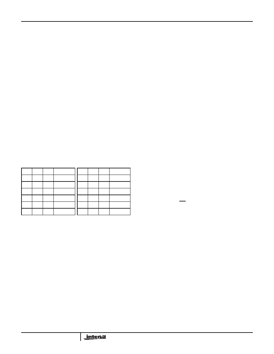
The output voltage span is controlled by 6 MSB’s of the
Configuration Register, which is at location 3Ch:
The 3 MSB’s control the VH span from 0.605V to 3.025V,
and the next three bits control the VL span from 0.151V
to 2.42V. Note that the selection of a value for VH can
never be lower than that for VL. Regardless of the range
selection, the specified linearity is guaranteed. Thus, if a
particular application requires operation from, say, 1.9V
to 2.4V, then the X79000 can be set for the range of
1.815V to 2.420V, yielding an LSB step size of 148V. If
a standard DAC were used with a 2.5V reference, then it
would need 14 bits of resolution to get the same LSB
step size.
The VH and VL pins can be used to monitor the selected
reference voltage, or as inputs for external reference
voltages. If an external voltage is to be applied to the VH
or the VL pins, the Configuration Register must be set to
value 000b for that reference to enable the external
reference setting (see Table 1). An externally applied
reference voltage can be time-varying, but the bandwidth
of the device will limit its use as a multiplying DAC to less
than 50kHz or so. The maximum voltage at the VH or VL
pins is 3.1V. Note that although VH and VL can be used
as inputs, the Reference pin (Vref) can only be used as
an output.
The Configuration Register is a non-volatile register, so
when a new VH or VL value is loaded it will be
remembered each time the device is powered up after a
power-down. This function is independent of the status of
the NVDAC bit, which is used only for the DAC registers.
Output Buffer (X79000, X79001 only)
Note that although the voltage span as determined by VH
is limited to +3.1V max, the output buffer can drive
voltages within 150mV of the positive rail. For a 5V ±5%
VCC supply, the DAC can have an output range up to
(4.75 - 0.150V) = 4.60V. The buffer would need a gain >1
set by adding feedback resistors to the Vbuf and VFB
pins, depending on the VH voltage.
For applications requiring voltages greater than 5V,
Intersil recommends the X79002 plus an external buffer.
UP/DOWN Operation
The UP/DOWN functionality of the chip uses the external
pins UP, DOWN, CS and CLR, and also the 2 LSB’s of
register 3Ch. The interface is designed to step up or
down by the increments set in register 3Ch. When 12-bit
operation is selected, then the LSB of the device (DAC0)
will increment or decrement with the appropriate pin
action. When 10-bit operation is selected, then third LSB
of the device (DAC2) will change, while leaving the two
LSB’s unchanged. When 8-bit operation is selected, then
the fifth LSB of the device (DAC4) will change, an and
the 4 LSB’s are unchanged. These options allow the
device to be used as either a 12-bit, 10-bit, or 8-bit DAC
for UP/DOWN applications. The X79000 UP/DOWN
interface allows stepping at up to 500kHz rates.
The CLR pin enables resetting the DAC output register to
all zeroes and can be used to initialize the DAC before
UP/DOWN operation.
VH2 VH1 VH0
Value
VL2 VL1 VL0
Value
0
external
0
external
0
1
605mV
0
1
151mV
01
0
1.21V
01
0
605mV
0
1
1.815V
0
1
1.21V
10
0
2.42V
10
0
1.815V
1
0
1
3.025V
1
0
1
2.42V
X79000, X79001, X79002
相关PDF资料 |
PDF描述 |
|---|---|
| B37941K5472K060 | CAP CER 4700PF 50V 10% X7R 0805 |
| X79000V20IT1 | IC DAC NV SELECT OUT/MEM 20TSSOP |
| VE-J6B-MW-F1 | CONVERTER MOD DC/DC 95V 100W |
| B37931K9223K060 | CAP CER 0.022UF 16V 10% X7R 0603 |
| X79000V20I | IC DAC NV SELECT OUT/MEM 20TSSOP |
相关代理商/技术参数 |
参数描述 |
|---|---|
| X79001V20IT1 | 功能描述:IC DAC NV SELECT OUT/MEM 20TSSOP RoHS:否 类别:集成电路 (IC) >> 数据采集 - 数模转换器 系列:- 标准包装:2,400 系列:- 设置时间:- 位数:18 数据接口:串行 转换器数目:3 电压电源:模拟和数字 功率耗散(最大):- 工作温度:-40°C ~ 85°C 安装类型:表面贴装 封装/外壳:36-TFBGA 供应商设备封装:36-TFBGA 包装:带卷 (TR) 输出数目和类型:* 采样率(每秒):* |
| X79002 | 制造商:INTERSIL 制造商全称:Intersil Corporation 功能描述:NV DAC with Selectable Output Range and Memory |
| X79002V20I | 功能描述:IC DAC NV SELECT OUT/MEM 20TSSOP RoHS:否 类别:集成电路 (IC) >> 数据采集 - 数模转换器 系列:- 标准包装:2,400 系列:- 设置时间:- 位数:18 数据接口:串行 转换器数目:3 电压电源:模拟和数字 功率耗散(最大):- 工作温度:-40°C ~ 85°C 安装类型:表面贴装 封装/外壳:36-TFBGA 供应商设备封装:36-TFBGA 包装:带卷 (TR) 输出数目和类型:* 采样率(每秒):* |
| X79002V20IT1 | 功能描述:IC DAC NV SELECT OUT/MEM 20TSSOP RoHS:否 类别:集成电路 (IC) >> 数据采集 - 数模转换器 系列:- 标准包装:2,400 系列:- 设置时间:- 位数:18 数据接口:串行 转换器数目:3 电压电源:模拟和数字 功率耗散(最大):- 工作温度:-40°C ~ 85°C 安装类型:表面贴装 封装/外壳:36-TFBGA 供应商设备封装:36-TFBGA 包装:带卷 (TR) 输出数目和类型:* 采样率(每秒):* |
| X790A | 制造商:STMICROELECTRONICS 制造商全称:STMicroelectronics 功能描述:Medium current, high performance, low voltage PNP transistor |
发布紧急采购,3分钟左右您将得到回复。