- 您现在的位置:买卖IC网 > PDF目录16197 > X90100EVAL (Intersil)EVALUATION BOARD DIGITAL CAPACIT PDF资料下载
参数资料
| 型号: | X90100EVAL |
| 厂商: | Intersil |
| 文件页数: | 5/7页 |
| 文件大小: | 0K |
| 描述: | EVALUATION BOARD DIGITAL CAPACIT |
| 标准包装: | 1 |
| 主要目的: | 数字电容器 |
| 已用 IC / 零件: | X90100 |
| 已供物品: | 板 |
5
FN8156.0
February 2, 2005
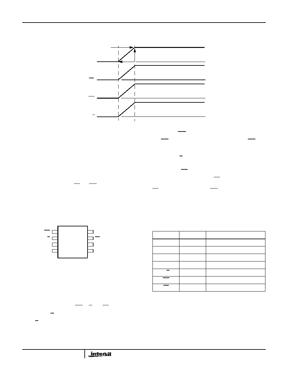
Power Up Timing (Digital Inputs Floating, Internal Pullup Action Shown)
Power Up and Down Requirements
There are no restrictions on the power-up or power-down
conditions of VCC and the voltages applied to the Cp, Cm
pins provided that VCC is always more positive than or equal
to VCp, VCm, i.e., VCC ≥ VCp, VCm. The VCC ramp rate spec
is always in effect.
Powerup Requirements
In order to prevent unwanted tap position changes or an
inadvertant store, bring the CS and INC high before or
concurrently with the VCC pin. The logic inputs have internal
active pullups to provide reliable powerup operation. See
powerup timing diagram.
Pin Configuration
Detailed Pin Descriptions
Cp and Cm
The high (Cp) and low (Cm) terminals of the X90100 are
equivalent to the fixed terminals of a mechanical trimmable
capacitor. The minimum dc voltage is VSS and the maximum
is VCC. The value of capacitance across the terminals is
determined by digital inputs INC, U/D, and CS.
Up/Down (U/D)
The U/D input controls the direction of the trimmed capacitor
value and whether the counter is incremented or
decremented. This pin has an active current source pullup.
Increment (INC)
The INC input is negative-edge triggered. Toggling INC will
move the capacitance value and either increment or
decrement the counter in the direction indicated by the logic
level on the U/D input. This pin has an active current source
pullup.
Chip Select (CS)
The device is selected when the CS input is LOW. The
current counter value is stored in nonvolatile memory when
CS is returned HIGH while the INC input is also HIGH. After
the store operation is complete the X90100 will be placed in
the low power standby mode until the device is selected
once again. This pin has active circuit source pullup.
N/C - This pin should be left floating.
Principles of Operation
There are three sections of the X90100: the input control,
counter and decode section; the nonvolatile memory; and
the capacitor array. The input control section operates just
like an up/down counter. The output of this counter is
decoded to turn on electronic switches connecting internal
units to the sum capacitor. Under the proper conditions the
contents of the counter can be stored in nonvolatile memory
VCC
CS
INC
U/D
VCC = 3.3 or 5.0V
tRVCC
VCC
CS
INC
U/D
1
2
3
4
8
7
6
5
X90100
MSOP
N/C (leave floating)
Cm
Vss
Cp
Pin Names
SYMBOL
DEFAULT
DESCRIPTION
Cp
output
Positive capacitor terminal
Cm
output
Negative capacitor terminal
VSS
supply
Ground
VCC
supply
Positive supply voltage
U/D
pull up
Up/Down control input
INC
pull up
Increment control input
CS
pull up
Chip Select control input
X90100
相关PDF资料 |
PDF描述 |
|---|---|
| GCM22DTBH | CONN EDGECARD 44POS R/A .156 SLD |
| GCM22DTBD | CONN EDGECARD 44POS R/A .156 SLD |
| GBM25DTAT | CONN EDGECARD 50POS R/A .156 SLD |
| GCM22DTAN | CONN EDGECARD 44POS R/A .156 SLD |
| APX825A-26W6G-7 | IC SUPERVISOR LO/HI 2.63V SOT-26 |
相关代理商/技术参数 |
参数描述 |
|---|---|
| X90100M8I | 功能描述:IC DIGITAL CAPACITOR NV 8-MSOP RoHS:否 类别:集成电路 (IC) >> 专用 IC 系列:- 产品培训模块:Lead (SnPb) Finish for COTS Obsolescence Mitigation Program 标准包装:1 系列:- 类型:调帧器 应用:数据传输 安装类型:表面贴装 封装/外壳:400-BBGA 供应商设备封装:400-PBGA(27x27) 包装:散装 |
| X90100M8IT1 | 功能描述:IC DIGITAL CAPACITOR NV 8-MSOP RoHS:否 类别:集成电路 (IC) >> 专用 IC 系列:- 产品培训模块:Lead (SnPb) Finish for COTS Obsolescence Mitigation Program 标准包装:1 系列:- 类型:调帧器 应用:数据传输 安装类型:表面贴装 封装/外壳:400-BBGA 供应商设备封装:400-PBGA(27x27) 包装:散装 |
| X90100M8IZ | 功能描述:射频无线杂项 32-TAP 7 5PF TO 14PF DIGTL CAPACITOR INT RoHS:否 制造商:Texas Instruments 工作频率:112 kHz to 205 kHz 电源电压-最大:3.6 V 电源电压-最小:3 V 电源电流:8 mA 最大功率耗散: 工作温度范围:- 40 C to + 110 C 封装 / 箱体:VQFN-48 封装:Reel |
| X90100M8IZT1 | 功能描述:射频无线杂项 32-TAP 7 5PF TO 14PF DIGTL CAPACITOR INT RoHS:否 制造商:Texas Instruments 工作频率:112 kHz to 205 kHz 电源电压-最大:3.6 V 电源电压-最小:3 V 电源电流:8 mA 最大功率耗散: 工作温度范围:- 40 C to + 110 C 封装 / 箱体:VQFN-48 封装:Reel |
| X90100MI | 制造商:XICOR 制造商全称:Xicor Inc. 功能描述:NV Electronically Programmable Capacitor |
发布紧急采购,3分钟左右您将得到回复。