参数资料
| 型号: | X9110TV14I-2.7 |
| 厂商: | Intersil |
| 文件页数: | 12/18页 |
| 文件大小: | 0K |
| 描述: | IC XDCP SGL 1024TAP 100K 14TSSOP |
| 标准包装: | 95 |
| 系列: | XDCP™ |
| 接片: | 1024 |
| 电阻(欧姆): | 100k |
| 电路数: | 1 |
| 温度系数: | 标准值 ±300 ppm/°C |
| 存储器类型: | 非易失 |
| 接口: | 4 线 SPI(芯片选择,设备位址) |
| 电源电压: | 2.7 V ~ 5.5 V |
| 工作温度: | -40°C ~ 85°C |
| 安装类型: | 表面贴装 |
| 封装/外壳: | 14-TSSOP(0.173",4.40mm 宽) |
| 供应商设备封装: | 14-TSSOP |
| 包装: | 管件 |
3
FN8158.3
February 13, 2008
Circuit Level Applications
Vary the gain of a voltage amplifier
Provide programmable dc reference voltages for
comparators and detectors
Control the volume in audio circuits
Trim out the offset voltage error in a voltage amplifier
circuit
Set the output voltage of a voltage regulator
Trim the resistance in Wheatstone bridge circuits
Control the gain, characteristic frequency and Q-factor in
filter circuits
Set the scale factor and zero point in sensor signal
conditioning circuits
Vary the frequency and duty cycle of timer ICs
Vary the dc biasing of a pin diode attenuator in RF circuits
Provide a control variable (I, V, or R) in feedback circuits
System Level Applications
Adjust the contrast in LCD displays
Control the power level of LED transmitters in
communication systems
Set and regulate the DC biasing point in an RF power
amplifier in wireless systems
Control the gain in audio and home entertainment systems
Provide the variable DC bias for tuners in RF wireless
systems
Set the operating points in temperature control systems
Control the operating point for sensors in industrial
systems
Trim offset and gain errors in artificial intelligent systems
Bus Interface Pins
SERIAL OUTPUT (SO)
SO is a serial data output pin. During a read cycle, data is
shifted out on this pin. Data is clocked out on the falling edge
of the serial clock.
SERIAL INPUT (SI)
SI is the serial data input pin. All opcodes, byte addresses
and data to be written to the pots and pot registers are input
on this pin. Data is latched by the rising edge of the serial
clock.
SERIAL CLOCK (SCK)
The SCK input is used to clock data into and out of the
X9110.
HOLD (HOLD)
HOLD is used in conjunction with the CS pin to select the
device. Once the part is selected and a serial sequence is
underway, HOLD may be used to pause the serial
communication with the controller without resetting the serial
sequence. To pause, HOLD must be brought LOW while SCK is
LOW. To resume communication, HOLD is brought HIGH, again
while SCK is LOW. If the pause feature is not used, HOLD should
be held HIGH at all times.
DEVICE ADDRESS (A0)
The address input is used to set the 8-bit slave address. A
match in the slave address serial data stream A0 must be
made with the address input (A0) in order to initiate
communication with the X9110.
CHIP SELECT (CS)
When CS is HIGH, the X9110 is deselected and the SO pin
is at high impedance, and (unless an internal write cycle is
underway) the device will be in the standby state. CS LOW
enables the X9110, placing it in the active power mode. It
should be noted that after a power-up, a HIGH to LOW
transition on CS is required prior to the start of any
operation.
HARDWARE WRITE PROTECT INPUT (WP)
The WP pin when LOW prevents nonvolatile writes to the
Data Registers.
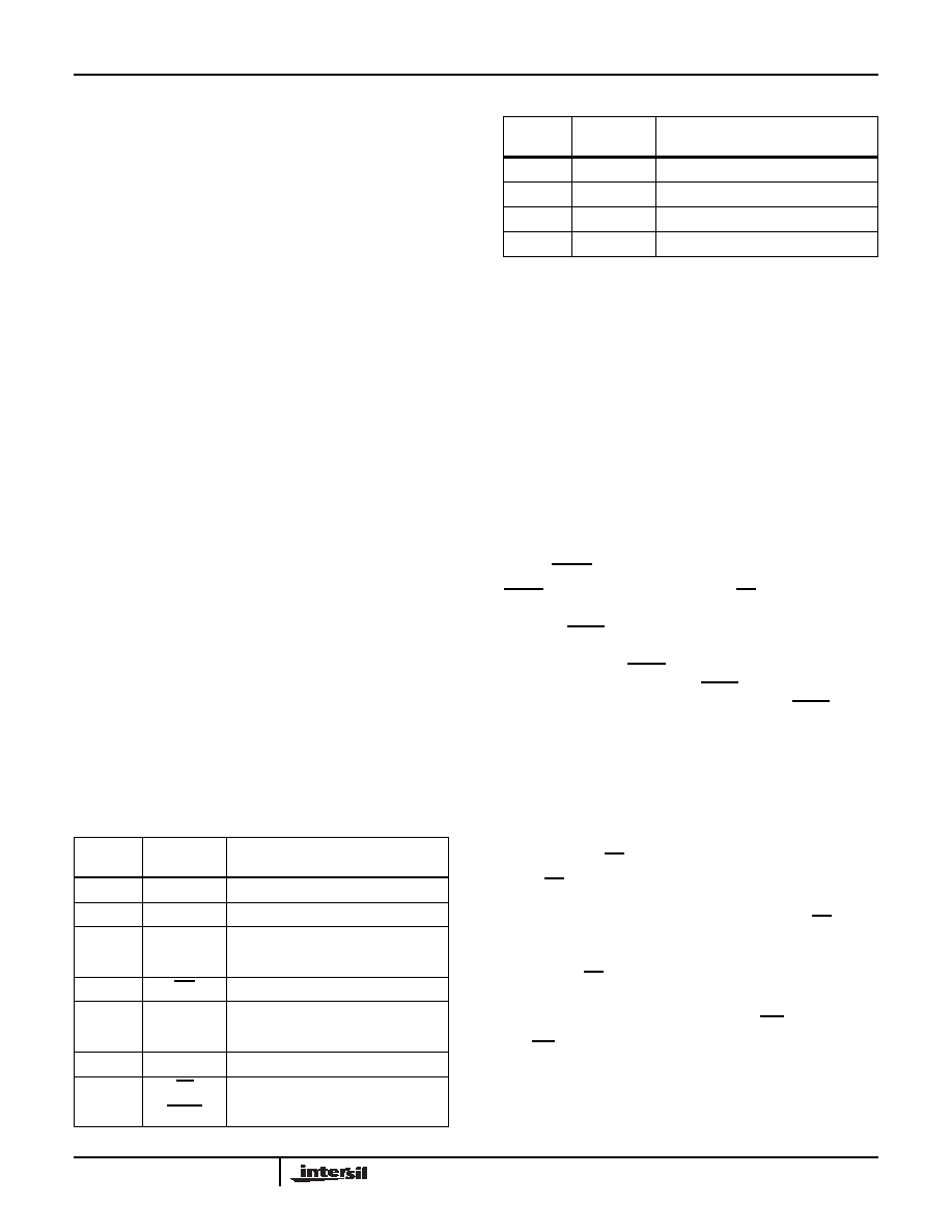
Pin Descriptions
PIN
(TSSOP)
SYMBOL
FUNCTION
1
V+
Analog Supply Voltage
2
SO
Serial Data Output
3
A0
Device Address
4
SCK
Serial Clock
5WP
Hardware Write Protect
6
SI
Serial Data Input
7VSS
System Ground
8V
-
Analog Supply Voltage
9CS
Chip Select
10
HOLD
Device Select. Pause the Serial Bus
11
RW
Wiper Terminal of the Potentiometer
12
RH
High Terminal of the Potentiometer
13
RL
Low Terminal of the Potentiometer
14
VCC
System Supply Voltage
Pin Descriptions (Continued)
PIN
(TSSOP)
SYMBOL
FUNCTION
X9110
相关PDF资料 |
PDF描述 |
|---|---|
| X9111TV14I-2.7T1 | IC XDCP SGL 1024TAP 100K 14TSSOP |
| X9116WS8T2 | IC XDCP 16-TAP 10K CMOS 8-SOIC |
| X9118TV14I-2.7 | IC XDCP SGL 1024TAP 100K 14TSSOP |
| X9119TV14-2.7T1 | IC XDCP SGL 1024TAP 100K 14TSSOP |
| X9221AYST2 | IC XDCP DUAL 2K 2-WIRE 20-SOIC |
相关代理商/技术参数 |
参数描述 |
|---|---|
| X9110TV14IZ | 功能描述:IC XDCP SGL 1024TAP 100K 14TSSOP RoHS:是 类别:集成电路 (IC) >> 数据采集 - 数字电位器 系列:XDCP™ 产品培训模块:Lead (SnPb) Finish for COTS Obsolescence Mitigation Program 标准包装:2,500 系列:- 接片:256 电阻(欧姆):100k 电路数:2 温度系数:标准值 35 ppm/°C 存储器类型:易失 接口:6 线串行(芯片选择,递增,增/减) 电源电压:2.6 V ~ 5.5 V 工作温度:-40°C ~ 125°C 安装类型:表面贴装 封装/外壳:14-TSSOP(0.173",4.40mm 宽) 供应商设备封装:14-TSSOP 包装:带卷 (TR) |
| X9110TV14IZ-2.7 | 功能描述:IC POT DGTL 100K OHM 14-TSSOP RoHS:是 类别:集成电路 (IC) >> 数据采集 - 数字电位器 系列:XDCP™ 产品培训模块:Lead (SnPb) Finish for COTS Obsolescence Mitigation Program 标准包装:1 系列:- 接片:256 电阻(欧姆):100k 电路数:1 温度系数:标准值 35 ppm/°C 存储器类型:非易失 接口:3 线串口 电源电压:2.7 V ~ 5.25 V 工作温度:-40°C ~ 85°C 安装类型:表面贴装 封装/外壳:8-WDFN 裸露焊盘 供应商设备封装:8-TDFN-EP(3x3) 包装:剪切带 (CT) 产品目录页面:1399 (CN2011-ZH PDF) 其它名称:MAX5423ETA+TCT |
| X9110TV14IZ-2.7T1 | 功能描述:IC XDCP 1024-TAP 100K 14-TSSOP RoHS:是 类别:集成电路 (IC) >> 数据采集 - 数字电位器 系列:XDCP™ 产品培训模块:Lead (SnPb) Finish for COTS Obsolescence Mitigation Program 标准包装:2,500 系列:- 接片:256 电阻(欧姆):100k 电路数:2 温度系数:标准值 35 ppm/°C 存储器类型:易失 接口:6 线串行(芯片选择,递增,增/减) 电源电压:2.6 V ~ 5.5 V 工作温度:-40°C ~ 125°C 安装类型:表面贴装 封装/外壳:14-TSSOP(0.173",4.40mm 宽) 供应商设备封装:14-TSSOP 包装:带卷 (TR) |
| X9110TV14Z | 功能描述:IC XDCP SGL 1024TAP 100K 14TSSOP RoHS:是 类别:集成电路 (IC) >> 数据采集 - 数字电位器 系列:XDCP™ 产品培训模块:Lead (SnPb) Finish for COTS Obsolescence Mitigation Program 标准包装:2,500 系列:- 接片:256 电阻(欧姆):100k 电路数:2 温度系数:标准值 35 ppm/°C 存储器类型:易失 接口:6 线串行(芯片选择,递增,增/减) 电源电压:2.6 V ~ 5.5 V 工作温度:-40°C ~ 125°C 安装类型:表面贴装 封装/外壳:14-TSSOP(0.173",4.40mm 宽) 供应商设备封装:14-TSSOP 包装:带卷 (TR) |
| X9110TV14Z-2.7 | 功能描述:IC XDCP SGL 1024TAP 100K 14TSSOP RoHS:是 类别:集成电路 (IC) >> 数据采集 - 数字电位器 系列:XDCP™ 产品培训模块:Lead (SnPb) Finish for COTS Obsolescence Mitigation Program 标准包装:2,500 系列:- 接片:256 电阻(欧姆):100k 电路数:2 温度系数:标准值 35 ppm/°C 存储器类型:易失 接口:6 线串行(芯片选择,递增,增/减) 电源电压:2.6 V ~ 5.5 V 工作温度:-40°C ~ 125°C 安装类型:表面贴装 封装/外壳:14-TSSOP(0.173",4.40mm 宽) 供应商设备封装:14-TSSOP 包装:带卷 (TR) |
发布紧急采购,3分钟左右您将得到回复。