参数资料
| 型号: | X9250UV24IZ |
| 厂商: | Intersil |
| 文件页数: | 16/20页 |
| 文件大小: | 0K |
| 描述: | IC XDCP QUAD 256TP 50K 24-TSSOP |
| 产品培训模块: | Solutions for Industrial Control Applications |
| 标准包装: | 62 |
| 系列: | XDCP™ |
| 接片: | 256 |
| 电阻(欧姆): | 50k |
| 电路数: | 4 |
| 温度系数: | 标准值 ±300 ppm/°C |
| 存储器类型: | 非易失 |
| 接口: | 6 线 SPI(芯片选择,设备位址) |
| 电源电压: | 4.5 V ~ 5.5 V |
| 工作温度: | -40°C ~ 85°C |
| 安装类型: | 表面贴装 |
| 封装/外壳: | 24-TSSOP(0.173",4.40mm 宽) |
| 供应商设备封装: | 24-TSSOP |
| 包装: | 管件 |
5
FN8165.3
August 29, 2006
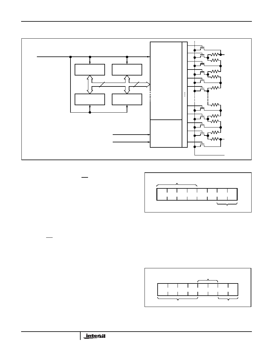
Figure 1. Detailed Potentiometer Block Diagram
Write in Process
The contents of the Data Registers are saved to
nonvolatile memory when the CS pin goes from LOW
to HIGH after a complete write sequence is received
by the device. The progress of this internal write
operation can be monitored by a write in process bit
(WIP). The WIP bit is read with a read status
command.
INSTRUCTIONS
Identification (ID) Byte
The first byte sent to the X9250 from the host,
following a CS going HIGH to LOW, is called the
Identification byte. The most significant four bits of the
slave address are a device type identifier, for the
X9250 this is fixed as 0101[B] (refer to Figure 2).
The two least significant bits in the ID byte select one
of four devices on the bus. The physical device
address is defined by the state of the A0 - A1 input
pins. The X9250 compares the serial data stream with
the address input state; a successful compare of both
address bits is required for the X9250 to successfully
continue the command sequence. The A0 - A1 inputs
can be actively driven by CMOS input signals or tied to
VCC or VSS.
The remaining two bits in the slave byte must be set to 0.
Figure 2. Identification Byte Format
Instruction Byte
The next byte sent to the X9250 contains the
instruction and register pointer information. The four
most significant bits are the instruction. The next four
bits point to one of the four pots and, when applicable,
they point to one of four associated registers. The
format is shown below in Figure 3.
Figure 3. Instruction Byte Format
Serial Data Path
From Interface
Circuitry
Register 0
Register 1
Register 2
Register 3
Serial
Bus
Input
Parallel
Input
Counter
Register
Inc/Dec
Logic
UP/DN
CLK
Modified SCK
UP/DN
VH/RH
VL/RL
VW/RW
88
C
o
u
n
t
e
r
D
e
c
o
d
e
If WCR = 00[H] then VW/RW = VL/RL
If WCR = FF[H] then VW/RW = VH/RH
Wiper
(One of Four Arrays)
(WCR)
Bus
1
00
0
A1
A0
Device Type
Identifier
Device Address
1
I1
I2
I3
I0
R1
R0
P1
P0
Pot Select
Register
Select
Instructions
X9250
相关PDF资料 |
PDF描述 |
|---|---|
| IDT728985J8 | IC DGTL SW 256X256 44-PLCC |
| VI-B1B-MW-F1 | CONVERTER MOD DC/DC 95V 100W |
| X9259UV24IZ | IC XDCP QUAD 256TAP 50K 24-TSSOP |
| IDT728980JG8 | IC DGTL SW 256X256 44-PLCC |
| SI4133-D-GT | IC SYNTHESIZR RF1/RF2/IF 24TSSOP |
相关代理商/技术参数 |
参数描述 |
|---|---|
| X9250UV24IZ-2.7 | 功能描述:IC XDCP QUAD 256TP 50K 24-TSSOP RoHS:是 类别:集成电路 (IC) >> 数据采集 - 数字电位器 系列:XDCP™ 产品培训模块:Lead (SnPb) Finish for COTS Obsolescence Mitigation Program 标准包装:2,500 系列:- 接片:256 电阻(欧姆):100k 电路数:2 温度系数:标准值 35 ppm/°C 存储器类型:易失 接口:6 线串行(芯片选择,递增,增/减) 电源电压:2.6 V ~ 5.5 V 工作温度:-40°C ~ 125°C 安装类型:表面贴装 封装/外壳:14-TSSOP(0.173",4.40mm 宽) 供应商设备封装:14-TSSOP 包装:带卷 (TR) |
| X9250UV24IZ-2.7T2 | 功能描述:IC XDCP QUAD 256TP 50K 24-TSSOP RoHS:是 类别:集成电路 (IC) >> 数据采集 - 数字电位器 系列:XDCP™ 产品培训模块:Lead (SnPb) Finish for COTS Obsolescence Mitigation Program 标准包装:2,500 系列:- 接片:256 电阻(欧姆):100k 电路数:2 温度系数:标准值 35 ppm/°C 存储器类型:易失 接口:6 线串行(芯片选择,递增,增/减) 电源电压:2.6 V ~ 5.5 V 工作温度:-40°C ~ 125°C 安装类型:表面贴装 封装/外壳:14-TSSOP(0.173",4.40mm 宽) 供应商设备封装:14-TSSOP 包装:带卷 (TR) |
| X9250UV24Z-2.7 | 制造商:INTERSIL 制造商全称:Intersil Corporation 功能描述:Quad Digitally Controlled Potentiometers |
| X9250UZ24 | 制造商:未知厂家 制造商全称:未知厂家 功能描述:DIGITAL POTENTIOMETER|CMOS|BGA|24PIN|PLASTIC |
| X9250UZ24-2.7 | 制造商:未知厂家 制造商全称:未知厂家 功能描述:DIGITAL POTENTIOMETER|CMOS|BGA|24PIN|PLASTIC |
发布紧急采购,3分钟左右您将得到回复。