参数资料
| 型号: | X9258TV24IZ-2.7 |
| 厂商: | Intersil |
| 文件页数: | 3/19页 |
| 文件大小: | 0K |
| 描述: | IC XDCP QUAD 256TP 100K 24TSSOP |
| 标准包装: | 62 |
| 系列: | XDCP™ |
| 接片: | 256 |
| 电阻(欧姆): | 100k |
| 电路数: | 4 |
| 温度系数: | 标准值 ±300 ppm/°C |
| 存储器类型: | 非易失 |
| 接口: | I²C(设备位址) |
| 电源电压: | 2.7 V ~ 5.5 V |
| 工作温度: | -40°C ~ 85°C |
| 安装类型: | 表面贴装 |
| 封装/外壳: | 24-TSSOP(0.173",4.40mm 宽) |
| 供应商设备封装: | 24-TSSOP |
| 包装: | 管件 |
11
FN8168.6
December 15, 2011
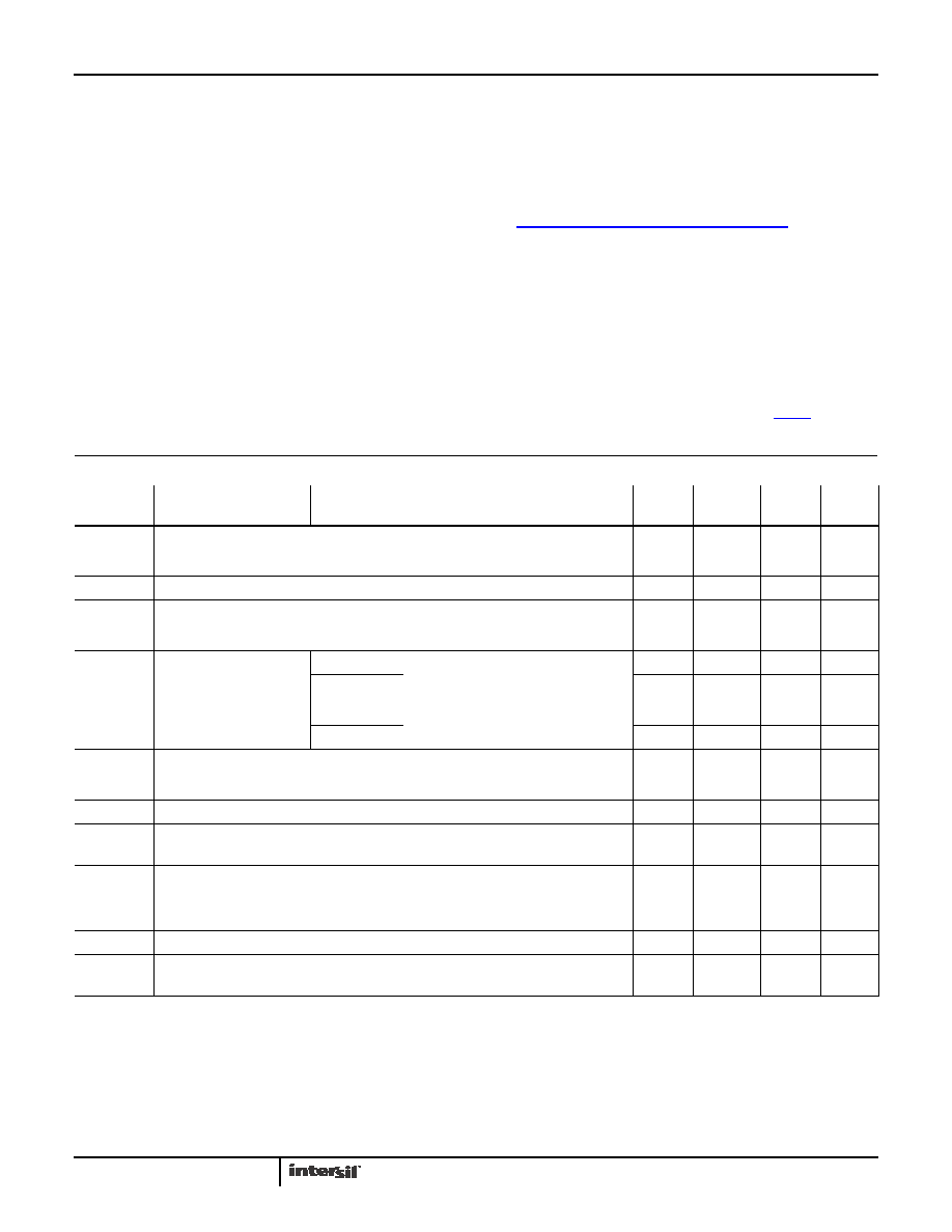
Absolute Maximum Ratings
Thermal Information
Voltage on SDA, SCL or any Address Input
with Respect to VSS . . . . . . . . . . . . . . . . . . . . . . . . . . . -1V to +7V
Voltage on V+ (referenced to VSS) . . . . . . . . . . . . . . . . . . . . . . .10V
Voltage on V- (referenced to VSS) . . . . . . . . . . . . . . . . . . . . . . . -10V
(V+) - (V-) . . . . . . . . . . . . . . . . . . . . . . . . . . . . . . . . . . . . . . . . . . .12V
Any VH/RH . . . . . . . . . . . . . . . . . . . . . . . . . . . . . . . . . . . . . . . . . . .V+
Any VL/RL . . . . . . . . . . . . . . . . . . . . . . . . . . . . . . . . . . . . . . . . . . . V-
IW (10s) . . . . . . . . . . . . . . . . . . . . . . . . . . . . . . . . . . . . . . . . . ±15mA
Thermal Resistance (Typical)
θJA (°C/W) θJC (°C/W)
24 Lead SOIC (Notes 10, 11). . . . . . . .
46
21
24 Lead TSSOP (Notes 10, 11) . . . . . .
68
17
Temperature Under Bias . . . . . . . . . . . . . . . . . . . . .-65°C to +135
°C
Storage Temperature . . . . . . . . . . . . . . . . . . . . . . . .-65
°C to +150°C
Pb-free Reflow Profile . . . . . . . . . . . . . . . . . . . . . . . . .see link below
Operating Conditions
Temperature Range . . . . . . . . . . . . . . . . . . . . . . . . . .-40°C to +85°C
Supply Voltage Range (Typical)
X9258. . . . . . . . . . . . . . . . . . . . . . . . . . . . . . . . . . . . . . . .5V ±10%
X9258-2.7. . . . . . . . . . . . . . . . . . . . . . . . . . . . . . . . . . 2.7V to 5.5V
CAUTION: Do not operate at or near the maximum ratings listed for extended periods of time. Exposure to such conditions may adversely impact product reliability and
result in failures not covered by warranty.
NOTES:
10.
θJA is measured with the component mounted on a high effective thermal conductivity test board in free air. See Tech Brief TB379 for details.
11. For
θJC, the “case temp” location is taken at the package top center.
Analog Specifications
Over recommended operating conditions, unless otherwise specified.
SYMBOL
PARAMETER
TEST CONDITIONS
MIN
(Note 12)
TYP
MAX
(Note 12)
UNIT
End-to-end Resistance Tolerance
±20
%
Power Rating
+25°C, each potentiometer
50
mW
IW
Wiper Current
Wiper current = ±1mA
±7.5
mA
RW
Wiper Resistance
IW = ± 1mA @ V+ = 3V, V- = -3V
150
250
RW
Wiper Resistance
IW = ± 1mA @ V+ = 5V, V- = -5V
40
100
V+
Voltage on V+ Pin
X9258
+4.5
+5.5
V
X9258-2.7
+2.7
+5.5
V
V-
Voltage on V- Pin
X9258
-5.5
-4.5
V
X9258 -2.7
-5.5
-2.7
V
VTERM
Voltage on any VH/RH or VL/RL Pin
V-
V+
V
Noise
Ref: 1kHz
-120
dBV
Resolution (Note 16)
0.6
%
Absolute Linearity (Note 13)
Vw(n)(actual) - Vw(n)(expected)
±1
MI
(Note 15)
Relative Linearity (Note 14)
Vw(n + 1) - [Vw(n) + MI]±0.6
MI
(Note 15)
Temperature Coefficient of RTOTAL
±300
ppm/
°C
Ratiometric Temperature Coefficient
±20
ppm/°C
CH/CL/CW Potentiometer Capacitance
10/10/25
pF
X9258
相关PDF资料 |
PDF描述 |
|---|---|
| MS3456W20-14S | CONN PLUG 5POS STRAIGHT W/SCKT |
| X9258US24IZ-2.7 | IC DGTL POT QUAD 100K 24SOIC |
| MS3456L20-14S | CONN PLUG 5POS STRAIGHT W/SCKT |
| X9258TS24IZ-2.7 | IC XDCP QUAD 256TP 100K 24-SOIC |
| VE-BWZ-MX-F4 | CONVERTER MOD DC/DC 2V 30W |
相关代理商/技术参数 |
参数描述 |
|---|---|
| X9258TV24Z-2.7 | 功能描述:IC XDCP QUAD 256TP 100K 24TSSOP RoHS:是 类别:集成电路 (IC) >> 数据采集 - 数字电位器 系列:XDCP™ 产品培训模块:Lead (SnPb) Finish for COTS Obsolescence Mitigation Program 标准包装:2,500 系列:- 接片:256 电阻(欧姆):100k 电路数:2 温度系数:标准值 35 ppm/°C 存储器类型:易失 接口:6 线串行(芯片选择,递增,增/减) 电源电压:2.6 V ~ 5.5 V 工作温度:-40°C ~ 125°C 安装类型:表面贴装 封装/外壳:14-TSSOP(0.173",4.40mm 宽) 供应商设备封装:14-TSSOP 包装:带卷 (TR) |
| X9258TZ24 | 制造商:未知厂家 制造商全称:未知厂家 功能描述:DIGITAL POTENTIOMETER|CMOS|BGA|24PIN|PLASTIC |
| X9258TZ24-2.7 | 制造商:未知厂家 制造商全称:未知厂家 功能描述:DIGITAL POTENTIOMETER|CMOS|BGA|24PIN|PLASTIC |
| X9258TZ24I | 制造商:未知厂家 制造商全称:未知厂家 功能描述:DIGITAL POTENTIOMETER|CMOS|BGA|24PIN|PLASTIC |
| X9258TZ24I-2.7 | 制造商:未知厂家 制造商全称:未知厂家 功能描述:DIGITAL POTENTIOMETER|CMOS|BGA|24PIN|PLASTIC |
发布紧急采购,3分钟左右您将得到回复。