- 您现在的位置:买卖IC网 > PDF目录20664 > X9259EVAL (Intersil)EVAL BOARD FOR X9259 PDF资料下载
参数资料
| 型号: | X9259EVAL |
| 厂商: | Intersil |
| 文件页数: | 16/21页 |
| 文件大小: | 0K |
| 描述: | EVAL BOARD FOR X9259 |
| 标准包装: | 1 |
| 系列: | * |
4
FN8169.5
April 13, 2007
Pin Descriptions
Bus Interface Pins
SERIAL DATA INPUT/OUTPUT (SDA)
The SDA is a bidirectional serial data input/output pin for a 2-
Wire slave device and is used to transfer data into and out of
the device. It receives device address, opcode, wiper
register address and data sent from a 2-Wire master at the
rising edge of the serial clock SCL, and it shifts out data after
each falling edge of the serial clock SCL.
It is an open drain output and may be wire-ORed with any
number of open drain or open collector outputs. An open
drain output requires the use of a pull-up resistor.
SERIAL CLOCK (SCL)
This input is used by 2-Wire master to supply 2-Wire serial
clock to the X9259.
DEVICE ADDRESS (A3 THROUGH A0)
The Address inputs are used to set the least significant 4 bits
of the 8-bit slave address. A match in the slave address
serial data stream must be made with the Address input in
order to initiate communication with the X9259. A maximum
of 16 devices may occupy the 2-Wire serial bus. Device pins
A3 through A0 must be tied to a logic level which specifies
Potentiometer Pins
RH, RL
The RH and RL pins are equivalent to the terminal
connections on a mechanical potentiometer. Since there are
4 potentiometers, there are 4 sets of RH and RL such that
RH0 and RL0 are the terminals of DCP0 and so on.
RW
The wiper pin are equivalent to the wiper terminal of a
mechanical potentiometer. Since there are 4 potentiometers,
there are 4 sets of RW such that RW0 is the terminal of
DCP0 and so on.
Bias Supply Pins
SYSTEM SUPPLY VOLTAGE (VCC) AND SUPPLY
GROUND (VSS)
The VCC pin is the system supply voltage. The VSS pin is
the system ground.
Other Pins
NO CONNECT
No connect pins should be left open. This pins are used for
Intersil manufacturing and testing purposes.
HARDWARE WRITE PROTECT INPUT (WP)
The WP pin when LOW prevents non-volatile writes to the
Data Registers.
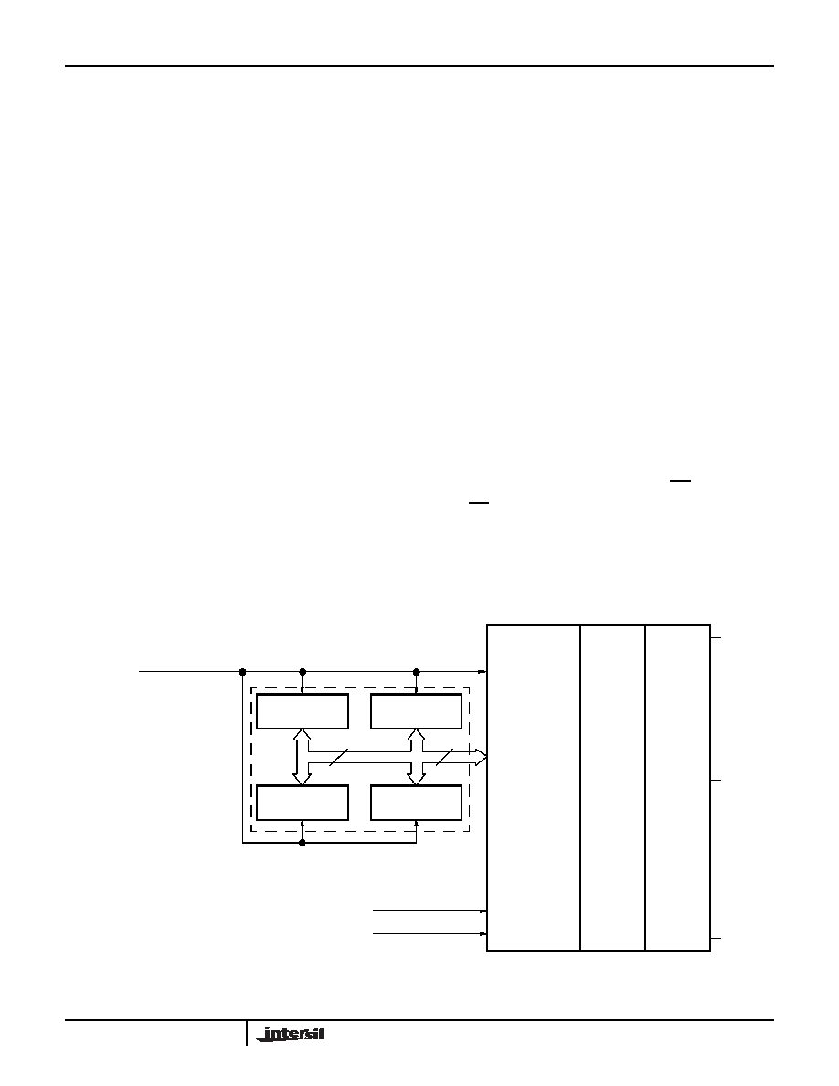
SERIAL DATA PATH
FROM INTERFACE
CIRCUITRY
DR#0
SERIAL
BUS
INPUT
PARALLEL
BUS
INPUT
COUNTER
REGISTER
INC/DEC
LOGIC
UP/DN
CLK
MODIFIED SCK
UP/DN
8
COUNTER
IF WCR = 00[H] then RW is closest to RL
IF WCR = FF[H] then RW is closest to RH
WIPER
(WCR#)
#: 0, 1, 2, or 3
One of Four Potentiometers
DR#2
DR#1
DR#3
- - -
DECODE
DCP
CORE
RW
RH
RL
FIGURE 1. DETAILED POTENTIOMETER BLOCK DIAGRAM
X9259
相关PDF资料 |
PDF描述 |
|---|---|
| ACM44DRKH | CONN EDGECARD 88POS DIP .156 SLD |
| AMC20DRYH-S93 | CONN EDGECARD 40POS DIP .100 SLD |
| EEC43DRXS | CONN EDGECARD 86POS DIP .100 SLD |
| TTN1.25SV | 1 1/4" THERMASHIELD TUBE 250' |
| ISL6539EVAL2 | EVAL BOARD 2 FOR ISL6539 |
相关代理商/技术参数 |
参数描述 |
|---|---|
| X9259TB24 | 制造商:XICOR 制造商全称:Xicor Inc. 功能描述:Quad Digitally-Controlled (XDCP) Potentiometers |
| X9259TB24-2.7 | 制造商:XICOR 制造商全称:Xicor Inc. 功能描述:Quad Digitally-Controlled (XDCP) Potentiometers |
| X9259TB24I | 制造商:XICOR 制造商全称:Xicor Inc. 功能描述:Quad Digitally-Controlled (XDCP) Potentiometers |
| X9259TB24I-2.7 | 制造商:XICOR 制造商全称:Xicor Inc. 功能描述:Quad Digitally-Controlled (XDCP) Potentiometers |
| X9259TS24 | 功能描述:IC DCP QUAD 100K 256TP 24SOIC RoHS:否 类别:集成电路 (IC) >> 数据采集 - 数字电位器 系列:XDCP™ 标准包装:2,500 系列:XDCP™ 接片:256 电阻(欧姆):100k 电路数:1 温度系数:标准值 ±300 ppm/°C 存储器类型:非易失 接口:I²C(设备位址) 电源电压:2.7 V ~ 5.5 V 工作温度:0°C ~ 70°C 安装类型:表面贴装 封装/外壳:14-TSSOP(0.173",4.40mm 宽) 供应商设备封装:14-TSSOP 包装:带卷 (TR) |
发布紧急采购,3分钟左右您将得到回复。