参数资料
| 型号: | X9269US24-2.7 |
| 厂商: | Intersil |
| 文件页数: | 23/24页 |
| 文件大小: | 0K |
| 描述: | IC XDCP DUAL 256TAP 50K 24-SOIC |
| 标准包装: | 30 |
| 系列: | XDCP™ |
| 接片: | 256 |
| 电阻(欧姆): | 50k |
| 电路数: | 2 |
| 温度系数: | 标准值 ±300 ppm/°C |
| 存储器类型: | 非易失 |
| 接口: | I²C(设备位址) |
| 电源电压: | 2.7 V ~ 5.5 V |
| 工作温度: | 0°C ~ 70°C |
| 安装类型: | 表面贴装 |
| 封装/外壳: | 24-SOIC(0.295",7.50mm 宽) |
| 供应商设备封装: | 24-SOIC |
| 包装: | 管件 |
8
FN8173.4
April 17, 2007
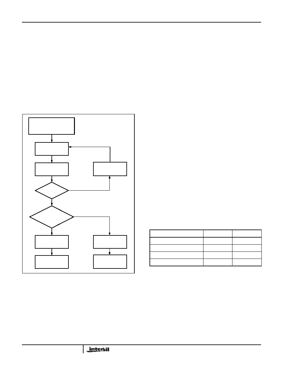
Acknowledge Polling
The disabling of the inputs, during the internal
nonvolatile write operation, can be used to take
advantage of the typical 5ms EEPROM write cycle
time. Once the stop condition is issued to indicate the
end of the nonvolatile write command the X9269
initiates the internal write cycle. ACK polling, Flow 1,
can be initiated immediately. This involves issuing the
start condition followed by the device slave address. If
the X9269 is still busy with the write operation no ACK
will be returned. If the X9269 has completed the write
operation an ACK will be returned and the master can
then proceed with the next operation.
FLOW 1: ACK Polling Sequence
INSTRUCTION AND REGISTER DESCRIPTION
Instructions
DEVICE ADDRESSING: IDENTIFICATION BYTE (ID AND A)
The first byte sent to the X9269 from the host is called
the Identification Byte. The most significant four bits of
the slave address are a device type identifier. The
ID[3:0] bits is the device id for the X9269; this is fixed
as 0101[B] (refer to Table 1).
The A[3:0] bits in the ID byte is the internal slave
address. The physical device address is defined by
the state of the A3-A0 input pins. The slave address
is externally specified by the user. The X9269
compares the serial data stream with the address
input state; a successful compare of both address
bits is required for the X9269 to successfully continue
the command sequence. Only the device which slave
address matches the incoming device address sent
by the master executes the instruction. The A3 - A0
inputs can be actively driven by CMOS input signals
or tied to VCC or VSS.
INSTRUCTION BYTE (I)
The next byte sent to the X9269 contains the
instruction and register pointer information. The three
most significant bits are used provide the instruction
opcode I [3:0]. The RB and RA bits point to one of the
four Data Registers of each associated XDCP. The
least significant bit points to one of two Wiper Counter
Registers or Pots. The format is shown in Table 2.
Register Selection
Nonvolatile Write
Command Completed
EnterACK Polling
Issue
START
Issue Slave
Address
ACK
Returned?
Further
Operation?
Issue
Instruction
Issue STOP
No
Yes
Proceed
Issue STOP
No
Proceed
Register Selected
RB
RA
DR0
0
DR1
0
1
DR2
1
0
DR3
1
X9269
相关PDF资料 |
PDF描述 |
|---|---|
| VI-26Y-MU-S | CONVERTER MOD DC/DC 3.3V 132W |
| X9269TV24 | IC XDCP DUAL 256TAP 100K 24TSSOP |
| VI-26T-MW-S | CONVERTER MOD DC/DC 6.5V 100W |
| VE-B7Y-MX-F1 | CONVERTER MOD DC/DC 3.3V 49.5W |
| X9269TS24T1 | IC XDCP DUAL 256TAP 100K 24-SOIC |
相关代理商/技术参数 |
参数描述 |
|---|---|
| X9269US24I | 功能描述:IC XDCP DUAL 256TAP 50K 24-SOIC RoHS:否 类别:集成电路 (IC) >> 数据采集 - 数字电位器 系列:XDCP™ 标准包装:2,500 系列:XDCP™ 接片:256 电阻(欧姆):100k 电路数:1 温度系数:标准值 ±300 ppm/°C 存储器类型:非易失 接口:I²C(设备位址) 电源电压:2.7 V ~ 5.5 V 工作温度:0°C ~ 70°C 安装类型:表面贴装 封装/外壳:14-TSSOP(0.173",4.40mm 宽) 供应商设备封装:14-TSSOP 包装:带卷 (TR) |
| X9269US24I-2.7 | 功能描述:IC XDCP DUAL 256TAP 50K 24-SOIC RoHS:否 类别:集成电路 (IC) >> 数据采集 - 数字电位器 系列:XDCP™ 标准包装:2,500 系列:XDCP™ 接片:256 电阻(欧姆):100k 电路数:1 温度系数:标准值 ±300 ppm/°C 存储器类型:非易失 接口:I²C(设备位址) 电源电压:2.7 V ~ 5.5 V 工作温度:0°C ~ 70°C 安装类型:表面贴装 封装/外壳:14-TSSOP(0.173",4.40mm 宽) 供应商设备封装:14-TSSOP 包装:带卷 (TR) |
| X9269US24I-2.7T1 | 功能描述:IC XDCP DUAL 256TAP 50K 24-SOIC RoHS:否 类别:集成电路 (IC) >> 数据采集 - 数字电位器 系列:XDCP™ 标准包装:2,500 系列:XDCP™ 接片:256 电阻(欧姆):100k 电路数:1 温度系数:标准值 ±300 ppm/°C 存储器类型:非易失 接口:I²C(设备位址) 电源电压:2.7 V ~ 5.5 V 工作温度:0°C ~ 70°C 安装类型:表面贴装 封装/外壳:14-TSSOP(0.173",4.40mm 宽) 供应商设备封装:14-TSSOP 包装:带卷 (TR) |
| X9269US24I-T/R | 制造商:Intersil Corporation 功能描述: |
| X9269US24IT1 | 功能描述:IC XDCP DUAL 256TAP 50K 24-SOIC RoHS:否 类别:集成电路 (IC) >> 数据采集 - 数字电位器 系列:XDCP™ 标准包装:2,500 系列:XDCP™ 接片:256 电阻(欧姆):100k 电路数:1 温度系数:标准值 ±300 ppm/°C 存储器类型:非易失 接口:I²C(设备位址) 电源电压:2.7 V ~ 5.5 V 工作温度:0°C ~ 70°C 安装类型:表面贴装 封装/外壳:14-TSSOP(0.173",4.40mm 宽) 供应商设备封装:14-TSSOP 包装:带卷 (TR) |
发布紧急采购,3分钟左右您将得到回复。