参数资料
| 型号: | X9408WS24IZ-2.7 |
| 厂商: | Intersil |
| 文件页数: | 15/20页 |
| 文件大小: | 0K |
| 描述: | IC XDCP QUAD 64TAP 10K 24-SOIC |
| 标准包装: | 30 |
| 系列: | XDCP™ |
| 接片: | 64 |
| 电阻(欧姆): | 10k |
| 电路数: | 4 |
| 温度系数: | 标准值 ±300 ppm/°C |
| 存储器类型: | 非易失 |
| 接口: | I²C(设备位址) |
| 电源电压: | 2.7 V ~ 5.5 V |
| 工作温度: | -40°C ~ 85°C |
| 安装类型: | 表面贴装 |
| 封装/外壳: | 24-SOIC(0.295",7.50mm 宽) |
| 供应商设备封装: | 24-SOIC |
| 包装: | 管件 |
4
FN8191.4
January 15, 2009
Principals of Operation
The X9408 is a highly integrated microcircuit incorporating
four resistor arrays and their associated registers and
counters and the serial interface logic providing direct
communication between the host and the XDCP
potentiometers.
Serial Interface
The X9408 supports a bidirectional bus oriented protocol.
The protocol defines any device that sends data onto the
bus as a transmitter and the receiving device as the receiver.
The device controlling the transfer is a master and the
device being controlled is the slave. The master will always
initiate data transfers and provide the clock for both transmit
and receive operations. Therefore, the X9408 will be
considered a slave device in all applications.
Clock and Data Conventions
Data states on the SDA line can change only during SCL
LOW periods (tLOW). SDA state changes during SCL HIGH
are reserved for indicating start and stop conditions.
Start Condition
All commands to the X9408 are preceded by the start
condition, which is a HIGH to LOW transition of SDA while
SCL is HIGH (tHIGH). The X9408 continuously monitors the
SDA and SCL lines for the start condition and will not
respond to any command until this condition is met.
Stop Condition
All communications must be terminated by a stop condition,
which is a LOW to HIGH transition of SDA while SCL is
HIGH.
Acknowledge
Acknowledge is a software convention used to provide a
positive handshake between the master and slave devices
on the bus to indicate the successful receipt of data. The
transmitting device, either the master or the slave, will
release the SDA bus after transmitting eight bits. The master
generates a ninth clock cycle and during this period the
receiver pulls the SDA line LOW to acknowledge that it
successfully received the eight bits of data.
The X9408 will respond with an acknowledge after
recognition of a start condition and its slave address and
once again after successful receipt of the command byte. If
the command is followed by a data byte the X9408 will
respond with a final acknowledge.
Array Description
The X9408 is comprised of four resistor arrays. Each array
contains 63 discrete resistive segments that are connected
in series. The physical ends of each array are equivalent to
the fixed terminals of a mechanical potentiometer (RH and
RLinputs).
At both ends of each array and between each resistor
segment is a CMOS switch connected to the wiper (RW)
output. Within each individual array only one switch may be
turned on at a time. These switches are controlled by the
Wiper Counter Register (WCR). The six bits of the WCR are
decoded to select, and enable, one of sixty-four switches.
The WCR may be written directly, or it can be changed by
transferring the contents of one of four associated Data
Registers into the WCR. These Data Registers and the WCR
can be read and written by the host system.
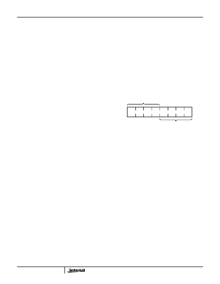
Device Addressing
Following a start condition the master must output the
address of the slave it is accessing. The most significant four
bits of the slave address are the device type identifier (refer
to Figure 1 below). For the X9408 this is fixed as 0101[B].
The next four bits of the slave address are the device
address. The physical device address is defined by the state
of the A0 - A3 inputs. The X9408 compares the serial data
stream with the address input state; a successful compare of
all four address bits is required for the X9408 to respond with
an acknowledge. The A0 - A3 inputs can be actively driven
by CMOS input signals or tied to VCC or VSS.
Acknowledge Polling
The disabling of the inputs, during the internal Nonvolatile
write operation, can be used to take advantage of the typical
5ms EEPROM write cycle time. Once the stop condition is
issued to indicate the end of the nonvolatile write command
the X9408 initiates the internal write cycle. ACK polling can
be initiated immediately. This involves issuing the start
condition followed by the device slave address. If the X9408
is still busy with the write operation no ACK will be returned.
If the X9408 has completed the write operation an ACK will
be returned and the master can then proceed with the next
operation.
1
00
A3
A2
A1
A0
DEVICE TYPE
IDENTIFIER
DEVICE ADDRESS
1
FIGURE 1. SLAVE ADDRESS
X9408
相关PDF资料 |
PDF描述 |
|---|---|
| V24A15H300BG | CONVERTER MOD DC/DC 15V 300W |
| IDTQS3VH16245PAG8 | IC BUS SWITCH 16BIT 48-TSSOP |
| M83723/75R20256 | CONN PLUG 25POS STRAIGHT W/SCKT |
| V24A15H300BF3 | CONVERTER MOD DC/DC 15V 300W |
| MS27467P25B61PD | CONN PLUG 61POS STRAIGHT W/PINS |
相关代理商/技术参数 |
参数描述 |
|---|---|
| X9408WS24M | 制造商:未知厂家 制造商全称:未知厂家 功能描述:Digital Potentiometer |
| X9408WS24M-2.7 | 制造商:未知厂家 制造商全称:未知厂家 功能描述:Digital Potentiometer |
| X9408WS24T1 | 功能描述:IC XDCP QUAD 64-TAP 10K 24-SOIC RoHS:否 类别:集成电路 (IC) >> 数据采集 - 数字电位器 系列:XDCP™ 产品培训模块:Lead (SnPb) Finish for COTS Obsolescence Mitigation Program 标准包装:2,500 系列:- 接片:32 电阻(欧姆):50k 电路数:1 温度系数:标准值 50 ppm/°C 存储器类型:易失 接口:3 线串行(芯片选择,递增,增/减) 电源电压:2.7 V ~ 5.5 V 工作温度:-40°C ~ 85°C 安装类型:表面贴装 封装/外壳:SOT-23-6 细型,TSOT-23-6 供应商设备封装:TSOT-23-6 包装:带卷 (TR) |
| X9408WSI-2.7 | 制造商:INTERSIL 制造商全称:Intersil Corporation 功能描述:Low Noise/Low Power/2-Wire Bus |
| X9408WV | 制造商:Intersil Corporation 功能描述: |
发布紧急采购,3分钟左右您将得到回复。