参数资料
| 型号: | X9421WV14ZT1 |
| 厂商: | Intersil |
| 文件页数: | 17/20页 |
| 文件大小: | 0K |
| 描述: | IC XDCP SGL 64-TAP 10K 14-TSSOP |
| 标准包装: | 2,500 |
| 系列: | XDCP™ |
| 接片: | 64 |
| 电阻(欧姆): | 10k |
| 电路数: | 1 |
| 温度系数: | 标准值 ±300 ppm/°C |
| 存储器类型: | 非易失 |
| 接口: | 5 线 SPI(芯片选择,设备位址) |
| 电源电压: | 4.5 V ~ 5.5 V |
| 工作温度: | 0°C ~ 70°C |
| 安装类型: | 表面贴装 |
| 封装/外壳: | 14-TSSOP(0.173",4.40mm 宽) |
| 供应商设备封装: | 14-TSSOP |
| 包装: | 带卷 (TR) |
6
FN8196.4
January 14, 2009
Write In Process
The contents of the Data Registers are saved to nonvolatile
memory when the CS pin goes from LOW to HIGH after a
complete write sequence is received by the device. The
progress of this internal write operation can be monitored by a
Write In Process bit (WIP). The WIP bit is read with a Read
Status command.
Instructions
Address/Identification (ID) Byte
The first byte sent to the X9421 from the host, following a CS
going HIGH to LOW, is called the Address or Identification
byte. The most significant four bits of the slave address are a
device type identifier, for the X9421 this is fixed as 0101[B]
(refer to Figure 2).
The least significant bit in the ID byte selects one of two
devices on the bus. The physical device address is defined
by the state of the A0 input pin. The X9421 compares the
serial data stream with the address input state; a successful
compare of the address bit is required for the X9421 to
successfully continue the command sequence. The A0 input
can be actively driven by a CMOS input signal or tied to VCC
or VSS.
The remaining three bits in the ID byte must be set to 110.
Instruction Byte
The next byte sent to the X9421 contains the instruction and
register pointer information. The four most significant bits are
the instruction. The next two bits point to one of four Data
Registers. The format is shown below in Figure 3.
The four high order bits of the instruction byte specify the
operation. The next two bits (R1 and R0) select one of the
four registers that is to be acted upon when a register
oriented instruction is issued. The last two bits are defined
as 0.
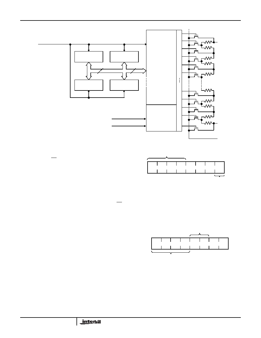
SERIAL DATA PATH
FROM INTERFACE
CIRCUITRY
REGISTER 0
REGISTER 1
REGISTER 2
REGISTER 3
SERIAL
BUS
INPUT
PARALLEL
BUS
INPUT
COUNTER
REGISTER
INC/DEC
LOGIC
UP/DN
CLK
MODIFIED SCK
UP/DN
VH
VL
VW
8
6
C
O
U
N
T
E
R
D
E
C
O
D
E
IF WCR = 00[H] THEN VW = VL
IF WCR = 3F[H] THEN VW = VH
WIPER
(WCR)
FIGURE 1. DETAILED POTENTIOMETER BLOCK DIAGRAM
1
0
11
0A0
DEVICE TYPE
IDENTIFIER
DEVICE ADDRESS
1
FIGURE 2. ADDRESS/IDENTIFICATION BYTE FORMAT
I1
I2
I3
I0
R1
R0
0
REGISTER
SELECT
INSTRUCTIONS
FIGURE 3. INSTRUCTION BYTE FORMAT
X9421
相关PDF资料 |
PDF描述 |
|---|---|
| VE-25Y-MW-F3 | CONVERTER MOD DC/DC 3.3V 66W |
| PI5C16245A | IC 16-BIT 4-PORT BUS SW 48-TSSOP |
| VE-25Y-MW-F2 | CONVERTER MOD DC/DC 3.3V 66W |
| VI-B4V-MV-S | CONVERTER MOD DC/DC 5.8V 150W |
| V300A5H300BG | CONVERTER MOD DC/DC 5V 300W |
相关代理商/技术参数 |
参数描述 |
|---|---|
| X9421WV-2.7 | 制造商:XICOR 制造商全称:Xicor Inc. 功能描述:Single Digitally Controlled (XDCP) Potentiometer |
| X9421WVI | 制造商:XICOR 制造商全称:Xicor Inc. 功能描述:Single Digitally Controlled (XDCP) Potentiometer |
| X9421WVI-2.7 | 制造商:XICOR 制造商全称:Xicor Inc. 功能描述:Single Digitally Controlled (XDCP) Potentiometer |
| X9421WW | 制造商:Intersil Corporation 功能描述:SINGLE XDCP, 10K OHM, 64 TAP, SPI, DIE/WAFER - Rail/Tube |
| X9421YP18I | 功能描述:IC XDCP SGL 64-TAP 2.5K 18-DIP RoHS:否 类别:集成电路 (IC) >> 数据采集 - 数字电位器 系列:XDCP™ 产品培训模块:Lead (SnPb) Finish for COTS Obsolescence Mitigation Program 标准包装:2,500 系列:- 接片:32 电阻(欧姆):50k 电路数:1 温度系数:标准值 50 ppm/°C 存储器类型:易失 接口:3 线串行(芯片选择,递增,增/减) 电源电压:2.7 V ~ 5.5 V 工作温度:-40°C ~ 85°C 安装类型:表面贴装 封装/外壳:SOT-23-6 细型,TSOT-23-6 供应商设备封装:TSOT-23-6 包装:带卷 (TR) |
发布紧急采购,3分钟左右您将得到回复。