参数资料
| 型号: | X9428WV14ZT1 |
| 厂商: | Intersil |
| 文件页数: | 18/21页 |
| 文件大小: | 0K |
| 描述: | IC DGTL POT 10K 1CH 14TSSOP |
| 标准包装: | 2,500 |
| 系列: | XDCP™ |
| 接片: | 64 |
| 电阻(欧姆): | 10k |
| 电路数: | 1 |
| 温度系数: | 标准值 ±300 ppm/°C |
| 存储器类型: | 非易失 |
| 接口: | 串行 |
| 电源电压: | 4.5 V ~ 5.5 V |
| 工作温度: | 0°C ~ 70°C |
| 安装类型: | 表面贴装 |
| 封装/外壳: | 14-TSSOP(0.173",4.40mm 宽) |
| 供应商设备封装: | 14-TSSOP |
| 包装: | 带卷 (TR) |
6
FN8197.1
April 26, 2006
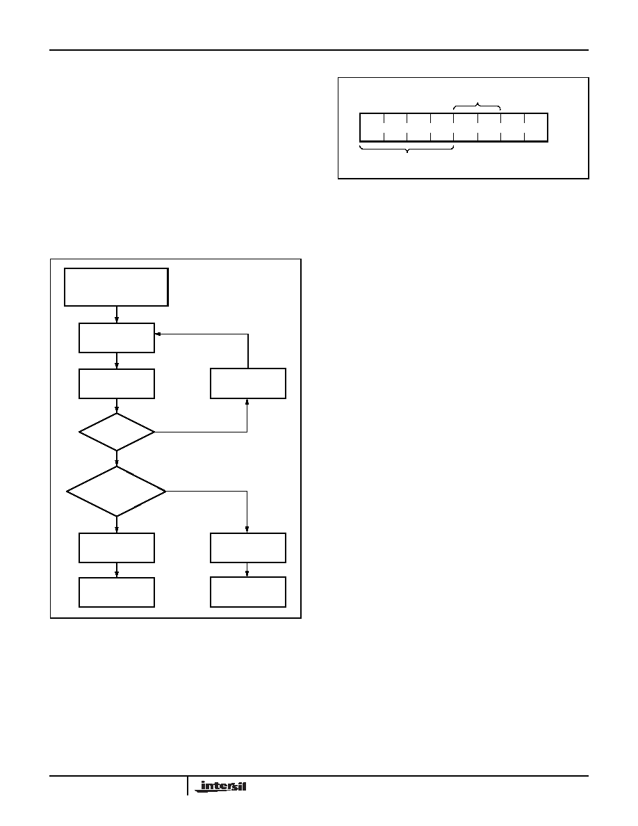
Acknowledge Polling
The disabling of the inputs, during the internal
nonvolatile write operation, can be used to take
advantage of the typical 5ms EEPROM write cycle
time. Once the stop condition is issued to indicate the
end of the nonvolatile write command the X9428
initiates the internal write cycle. ACK polling can be
initiated immediately. This involves issuing the start
condition followed by the device slave address. If the
X9428 is still busy with the write operation no ACK will
be returned. If the X9428 has completed the write
operation an ACK will be returned, and the master can
then proceed with the next operation.
Flow 1. ACK Polling Sequence
Instruction Structure
The next byte sent to the X9428 contains the instruction
and register pointer information. The four most
significant bits are the instruction. The next four bits
point to one of four associated registers. The format is
shown below in Figure 2.
Figure 2. Instruction Byte Format
The four high order bits define the instruction. The next
two bits (R1 and R0) select one of the four registers that
is to be acted upon when a register oriented instruction
is issued. Bits 0 and 1 are defined to be 0.
Four of the seven instructions end with the transmission
of the instruction byte. The basic sequence is illustrated
in Figure 3. These two-byte instructions exchange data
between the Wiper Counter Register and one of the
Data Registers. A transfer from a Data Register to a
Wiper Counter Register is essentially a write to a static
RAM. The response of the wiper to this action will be
delayed tWRL. A transfer from the Wiper Counter
Register (current wiper position), to a Data Register is a
write to nonvolatile memory and takes a minimum of
tWR to complete.
Four instructions require a three-byte sequence to
complete. These instructions transfer data between the
host and the X9428; either between the host and one of
the Data Registers or directly between the host and the
Wiper Counter Register. These instructions are: Read
Wiper Counter Register (read the current wiper position
of the selected pot), write Wiper Counter Register
(change current wiper position of the selected pot), read
Data Register (read the contents of the selected
nonvolatile register) and write Data Register (write a
new value to the selected Data Register). The
sequence of operations is shown in Figure 4.
Nonvolatile Write
Command Completed
Enter ACK Polling
Issue
START
Issue Slave
Address
ACK
Returned?
Further
Operation?
Issue
Instruction
Issue STOP
NO
YES
Proceed
Issue STOP
NO
Proceed
I1
I2
I3
I0
R1
R0
0
Register
Select
Instructions
X9428
相关PDF资料 |
PDF描述 |
|---|---|
| VI-B5J-MV-S | CONVERTER MOD DC/DC 36V 150W |
| VI-B53-MV-S | CONVERTER MOD DC/DC 24V 150W |
| M83723/75R24618 | CONN PLUG 61POS STRAIGHT W/SCKT |
| M83723/75R24617 | CONN PLUG 61POS STRAIGHT W/SCKT |
| M83723/75R24616 | CONN PLUG 61POS STRAIGHT W/SCKT |
相关代理商/技术参数 |
参数描述 |
|---|---|
| X9428WV-2.7 | 制造商:INTERSIL 制造商全称:Intersil Corporation 功能描述:Single Digitally Controlled Potentiometer |
| X9428WVI | 制造商:INTERSIL 制造商全称:Intersil Corporation 功能描述:Single Digitally Controlled Potentiometer |
| X9428WVI-2.7 | 制造商:INTERSIL 制造商全称:Intersil Corporation 功能描述:Single Digitally Controlled Potentiometer |
| X9428WVM | 制造商:未知厂家 制造商全称:未知厂家 功能描述:Industrial Control IC |
| X9428WVM2.7 | 制造商:未知厂家 制造商全称:未知厂家 功能描述:Industrial Control IC |
发布紧急采购,3分钟左右您将得到回复。