- 您现在的位置:买卖IC网 > PDF目录376449 > X9525V20I (INTERSIL CORP) Fiber Channel/Gigabit Etherner Laser Diode Control for Fiber Optic Modules PDF资料下载
参数资料
| 型号: | X9525V20I |
| 厂商: | INTERSIL CORP |
| 元件分类: | 数字电位计 |
| 英文描述: | Fiber Channel/Gigabit Etherner Laser Diode Control for Fiber Optic Modules |
| 中文描述: | DUAL 50K DIGITAL POTENTIOMETER, 2-WIRE SERIAL CONTROL INTERFACE, 256 POSITIONS, PDSO20 |
| 封装: | PLASTIC, TSSOP-20 |
| 文件页数: | 8/26页 |
| 文件大小: | 578K |
| 代理商: | X9525V20I |
8
FN8210.0
March 10, 2005
It should be noted that all writes to any DCP of the X9525
are random in nature. Therefore, the Data Byte of con-
secutive write operations to any DCP can differ by an
arbitrary number of bits. Also, setting the bits (P1 = 0,
P0 = 0) or (P1 = 1, P0 = 1) are reserved sequences, and
will result in no ACKNOWLEDGE after sending an
Instruction Byte on SDA.
The factory default setting of all “wiper position” settings
is with 00h stored in the NVM of the DCPs. This corre-
sponds to having the “wiper teminal”
R
WX
(x = 1,2) at the
“lowest” tap position, therefore, the resistance between
R
WX
and
R
LX
is a minimum (essentially only the Wiper
Resistance,
R
W
).
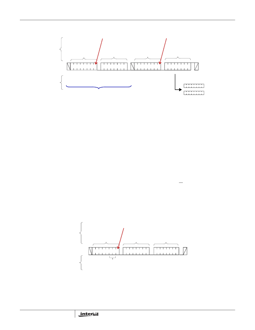
DCP Read Operation
A read of DCPx (x = 1,2) can be performed using the
three byte random read command sequence shown in
Figure 10.
The master issues the START condition and the Slave
Address Byte 1010A
0
110 which specifies that a
“dummy” write” is to be conducted. This “dummy” write
operation sets which DCP is to be read (in the preceding
Read operation). An ACKNOWLEDGE is returned by the
X9525 after the Slave Address if received correctly. Next,
an Instruction Byte is issued on SDA. Bits P1 - P0 of the
Instruction Byte determine which DCP “wiper position” is
to be read. In this case, the state of the WT bit is “don’t
care”. If the Instruction Byte format is valid, then another
ACKNOWLEDGE is returned by the X9525.
Following this ACKNOWLEDGE, the master immediately
issues another START condition and a valid Slave
address byte with the R/W bit set to 1. Then the X9525
issues an ACKNOWLEDGE followed by Data Byte, and
finally, the master issues a STOP condition. The Data
Byte read in this operation, corresponds to the “wiper
position” (value of the WCR) of the DCP pointed to by
bits P1 and P0.
Slave
Address
Instruction
Byte
A
C
K
A
C
K
S
t
a
r
t
S
t
o
p
Slave
Address
Data Byte
A
C
K
S
t
a
r
t
SDA Bus
Signals from
the Slave
Signals from
the Master
Figure 10. DCP Read Sequence
“Dummy” write
READ Operation
101
11
0
0
00 00
W
T
P
1
P
0
101
11
1
0
WRITE Operation
-
MSB
LSB
DCPx
x = 1
x = 2
“-” = DON’T CARE
A
0
A
0
S
t
a
r
t
S
t
o
p
Slave
Address
Address
Byte
Data
Byte
A
C
K
A
C
K
A
C
K
SDA Bus
Signals from
the Slave
Signals from
the Master
Figure 11. EEPROM Byte Write Sequence
Internal
Device
Address
1 0 1 0
00
0
WRITE Operation
A
0
X9525
相关PDF资料 |
PDF描述 |
|---|---|
| X9530 | Temperature Compensated Laser Diode Controller(带温度补偿的激光二极管控制器) |
| X95840 | Quad Digital Controlled Potentiometers |
| X95840WV20I-2.7 | Quad Digital Controlled Potentiometers |
| X95840UV20I-2.7 | Quad Digital Controlled Potentiometers |
| X95840WV20IZ-2.7 | Quad Digital Controlled Potentiometers |
相关代理商/技术参数 |
参数描述 |
|---|---|
| X9525V20IT1 | 功能描述:IC DCP DUAL EEPROM MEM 20-TSSOP RoHS:否 类别:集成电路 (IC) >> PMIC - 激光驱动器 系列:- 产品培训模块:Lead (SnPb) Finish for COTS Obsolescence Mitigation Program 标准包装:60 系列:- 类型:激光二极管驱动器 数据速率:- 通道数:4 电源电压:3.3V 电流 - 电源:- 电流 - 调制:- 电流 - 偏置:- 工作温度:0°C ~ 70°C 封装/外壳:40-TQFN 裸露焊盘 供应商设备封装:40-TQFN EP 包装:托盘 安装类型:表面贴装 |
| X9525V20IZ | 制造商:INTERSIL 制造商全称:Intersil Corporation 功能描述:Dual DCP, EEPROM Memory |
| X9530 | 制造商:INTERSIL 制造商全称:Intersil Corporation 功能描述:Temperature Compensated Laser Diode Controller |
| X9530_0511 | 制造商:INTERSIL 制造商全称:Intersil Corporation 功能描述:Temperature Compensated Laser Diode Controller |
| X9530B15I | 制造商:XICOR 制造商全称:Xicor Inc. 功能描述:Temperature Compensated Laser Diode Controller |
发布紧急采购,3分钟左右您将得到回复。