参数资料
| 型号: | X95820UV14I-2.7 |
| 厂商: | Intersil |
| 文件页数: | 3/12页 |
| 文件大小: | 0K |
| 描述: | IC XDCP DUAL 256TAP 50K 14-TSSOP |
| 标准包装: | 95 |
| 系列: | XDCP™ |
| 接片: | 256 |
| 电阻(欧姆): | 50k |
| 电路数: | 2 |
| 温度系数: | 标准值 ±45 ppm/°C |
| 存储器类型: | 非易失 |
| 接口: | I²C(设备位址) |
| 电源电压: | 2.7 V ~ 5.5 V |
| 工作温度: | -40°C ~ 85°C |
| 安装类型: | 表面贴装 |
| 封装/外壳: | 14-TSSOP(0.173",4.40mm 宽) |
| 供应商设备封装: | 14-TSSOP |
| 包装: | 管件 |
11
FN8212.2
July 18, 2006
Write Operation
A Write operation requires a START condition, followed by a
valid Identification Byte, a valid Address Byte, a Data Byte,
and a STOP condition. After each of the three bytes, the
X95820 responds with an ACK. At this time, if the Data Byte
is to be written only to volatile registers, then the device
enters its standby state. If the Data Byte is to be written also
to non-volatile memory, the X95820 begins its internal write
cycle to non-volatile memory. During the internal non-volatile
write cycle, the device ignores transitions at the SDA and
SCL pins, and the SDA output is at a high impedance state.
When the internal non-volatile write cycle is completed, the
X95820 enters its standby state (See Figure 17).
The byte at address 00001000 bin (8 decimal) determines if
the Data Byte is to be written to volatile and/or non-volatile
memory. See “Memory Description” on page 9.
Data Protection
The WP pin has to be at logic HIGH to perform any Write
operation to the device. When the WP is active (LOW) the
device ignores Data Bytes of a Write Operation, does not
respond to the Data Bytes with an ACK, and instead, goes to
its standby state waiting for a new START condition.
A STOP condition also acts as a protection of non-volatile
memory. A valid Identification Byte, Address Byte, and total
number of SCL pulses act as a protection of both volatile
and non-volatile registers. During a Write sequence, the
Data Byte is loaded into an internal shift register as it is
received. If the Address Byte is 0, 1, or 8 decimal, the Data
Byte is transferred to the appropriate Wiper Register (WR) or
to the Access Control Register, at the falling edge of the SCL
pulse that loads the last bit (LSB) of the Data Byte. If the
Address Byte is between 0 and 6 (inclusive), and the Access
Control Register is all zeros (default), then the STOP
condition initiates the internal write cycle to non-volatile
memory.
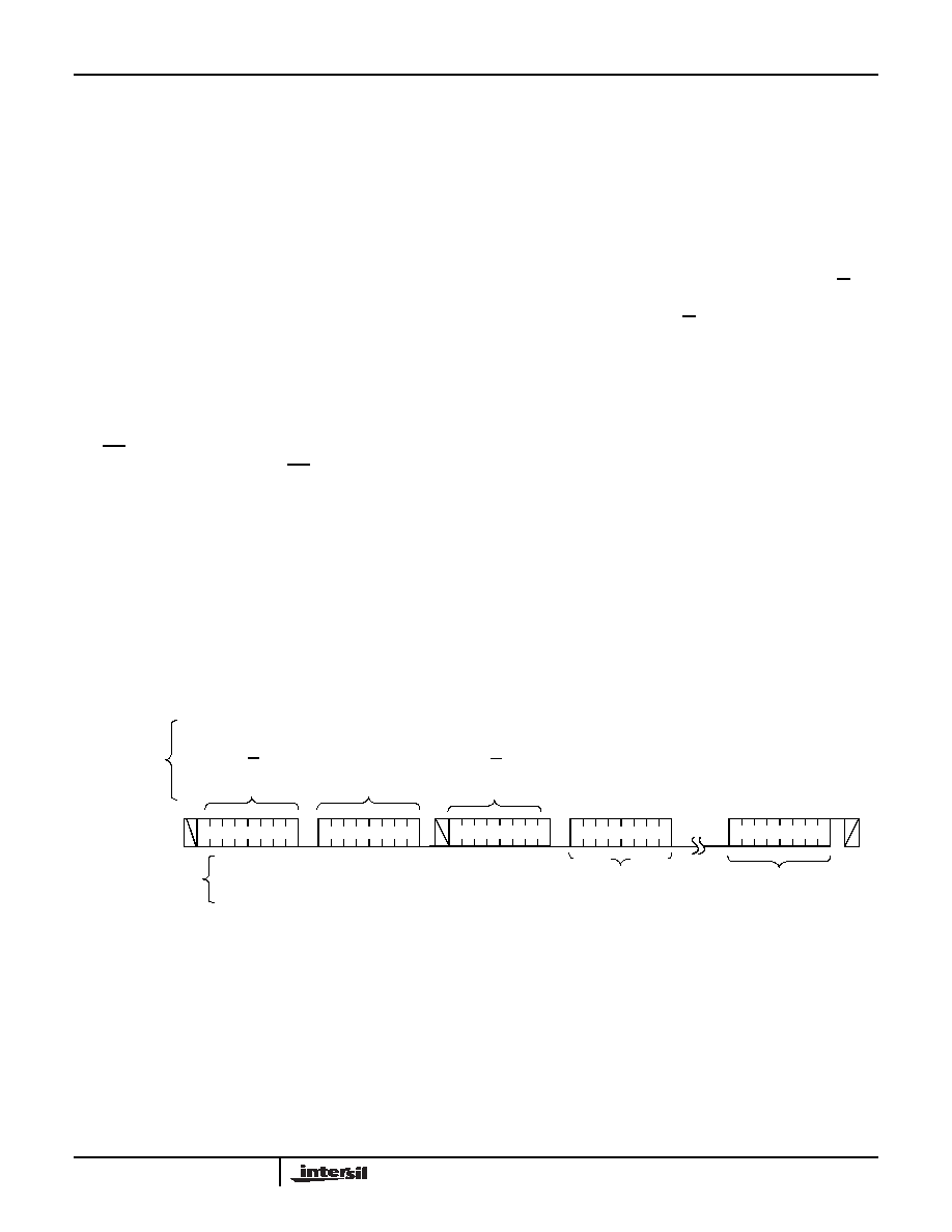
Read Operation
A Read operation consists of a three byte instruction
followed by one or more Data Bytes (See Figure 18). The
master initiates the operation issuing the following
sequence: a START, the Identification byte with the R/W bit
set to “0”, an Address Byte, a second START, and a second
Identification byte with the R/W bit set to “1”. After each of
the three bytes, the X95820 responds with an ACK. Then the
X95820 transmits Data Bytes as long as the master
responds with an ACK during the SCL cycle following the
eight bit of each byte. The master terminates the read
operation (issuing a STOP condition) following the last bit of
the last Data Byte (See Figure 18).
The Data Bytes are from the memory location indicated by
an internal pointer. This pointer initial value is determined by
the Address Byte in the Read operation instruction, and
increments by one during transmission of each Data Byte.
After reaching the memory location 01Fh (8 decimal) the
pointer “rolls over” to 00h, and the device continues to output
data for each ACK received.
The byte at address 00001000 bin (8 decimal) determines if
the Data Bytes being read are from volatile or non-volatile
memory. See “Memory Description” on page 9.
Signals
from the
Master
Signals from the
Slave
Signal at SDA
S
t
a
r
t
Identification
Byte
with
R/W=0
Address
Byte
A
C
K
A
C
K
1
0
1
00
S
t
o
p
A
C
K
1
00
Identification
Byte
with
R/W=1
A
C
K
S
t
a
r
t
Last Read Data
Byte
First Read Data
Byte
A
C
K
FIGURE 18. READ SEQUENCE
X95820
相关PDF资料 |
PDF描述 |
|---|---|
| VE-B4V-MV-S | CONVERTER MOD DC/DC 5.8V 150W |
| VE-B5P-MY-F1 | CONVERTER MOD DC/DC 13.8V 50W |
| IDT2308A-2DCG8 | IC CLOCK MULT ZD 3.3V 16-SOIC |
| VE-B5M-MY-F4 | CONVERTER MOD DC/DC 10V 50W |
| X9C303V8T1 | IC XDCP 100-TAP 32K EE 8-TSSOP |
相关代理商/技术参数 |
参数描述 |
|---|---|
| X95820UV14IZ-2.7 | 功能描述:IC XDCP DUAL 256TAP 50K 14-TSSOP RoHS:是 类别:集成电路 (IC) >> 数据采集 - 数字电位器 系列:XDCP™ 产品培训模块:Lead (SnPb) Finish for COTS Obsolescence Mitigation Program 标准包装:2,500 系列:- 接片:256 电阻(欧姆):100k 电路数:2 温度系数:标准值 35 ppm/°C 存储器类型:易失 接口:6 线串行(芯片选择,递增,增/减) 电源电压:2.6 V ~ 5.5 V 工作温度:-40°C ~ 125°C 安装类型:表面贴装 封装/外壳:14-TSSOP(0.173",4.40mm 宽) 供应商设备封装:14-TSSOP 包装:带卷 (TR) |
| X95820UV14IZ-2.7T1 | 功能描述:IC XDCP DUAL 256TAP 50K 14-TSSOP RoHS:是 类别:集成电路 (IC) >> 数据采集 - 数字电位器 系列:XDCP™ 产品培训模块:Lead (SnPb) Finish for COTS Obsolescence Mitigation Program 标准包装:2,500 系列:- 接片:256 电阻(欧姆):100k 电路数:2 温度系数:标准值 35 ppm/°C 存储器类型:易失 接口:6 线串行(芯片选择,递增,增/减) 电源电压:2.6 V ~ 5.5 V 工作温度:-40°C ~ 125°C 安装类型:表面贴装 封装/外壳:14-TSSOP(0.173",4.40mm 宽) 供应商设备封装:14-TSSOP 包装:带卷 (TR) |
| X95820WV14I-2.7 | 功能描述:IC XDCP DUAL 256TAP 10K 14-TSSOP RoHS:否 类别:集成电路 (IC) >> 数据采集 - 数字电位器 系列:XDCP™ 产品培训模块:Lead (SnPb) Finish for COTS Obsolescence Mitigation Program 标准包装:2,500 系列:- 接片:32 电阻(欧姆):50k 电路数:1 温度系数:标准值 50 ppm/°C 存储器类型:易失 接口:3 线串行(芯片选择,递增,增/减) 电源电压:2.7 V ~ 5.5 V 工作温度:-40°C ~ 85°C 安装类型:表面贴装 封装/外壳:SOT-23-6 细型,TSOT-23-6 供应商设备封装:TSOT-23-6 包装:带卷 (TR) |
| X95820WV14I-2.7T1 | 功能描述:IC XDCP DUAL 256TAP 10K 14-TSSOP RoHS:否 类别:集成电路 (IC) >> 数据采集 - 数字电位器 系列:XDCP™ 产品培训模块:Lead (SnPb) Finish for COTS Obsolescence Mitigation Program 标准包装:2,500 系列:- 接片:32 电阻(欧姆):50k 电路数:1 温度系数:标准值 50 ppm/°C 存储器类型:易失 接口:3 线串行(芯片选择,递增,增/减) 电源电压:2.7 V ~ 5.5 V 工作温度:-40°C ~ 85°C 安装类型:表面贴装 封装/外壳:SOT-23-6 细型,TSOT-23-6 供应商设备封装:TSOT-23-6 包装:带卷 (TR) |
| X95820WV14IZ-2.7 | 功能描述:IC XDCP DUAL 256TAP 10K 14-TSSOP RoHS:是 类别:集成电路 (IC) >> 数据采集 - 数字电位器 系列:XDCP™ 产品培训模块:Lead (SnPb) Finish for COTS Obsolescence Mitigation Program 标准包装:2,500 系列:- 接片:256 电阻(欧姆):100k 电路数:2 温度系数:标准值 35 ppm/°C 存储器类型:易失 接口:6 线串行(芯片选择,递增,增/减) 电源电压:2.6 V ~ 5.5 V 工作温度:-40°C ~ 125°C 安装类型:表面贴装 封装/外壳:14-TSSOP(0.173",4.40mm 宽) 供应商设备封装:14-TSSOP 包装:带卷 (TR) |
发布紧急采购,3分钟左右您将得到回复。