- 您现在的位置:买卖IC网 > PDF目录19899 > XC18V02VQG44C (Xilinx Inc)IC PROM REPROGR 2MB 44-VQFP PDF资料下载
参数资料
| 型号: | XC18V02VQG44C |
| 厂商: | Xilinx Inc |
| 文件页数: | 1/24页 |
| 文件大小: | 0K |
| 描述: | IC PROM REPROGR 2MB 44-VQFP |
| 标准包装: | 160 |
| 可编程类型: | 系统内可编程 |
| 存储容量: | 2Mb |
| 电源电压: | 3 V ~ 3.6 V |
| 工作温度: | 0°C ~ 70°C |
| 封装/外壳: | 44-TQFP |
| 供应商设备封装: | 44-VQFP(10x10) |
| 包装: | 托盘 |
DS026 (v5.2) January 11, 2008
Product Specification
1
1999–2008 Xilinx, Inc. All rights reserved. XILINX, the Xilinx logo, the Brand Window, and other designated brands included herein are trademarks of Xilinx, Inc. All other
trademarks are the property of their respective owners.
Features
In-System Programmable 3.3V PROMs for
Configuration of Xilinx FPGAs
Endurance of 20,000 Program/Erase Cycles
Program/Erase Over Full Industrial Voltage and
Temperature Range (–40
°C to +85°C)
IEEE Std 1149.1 Boundary-Scan (JTAG) Support
JTAG Command Initiation of Standard FPGA
Configuration
Simple Interface to the FPGA
Cascadable for Storing Longer or Multiple Bitstreams
Low-Power Advanced CMOS FLASH Process
Dual Configuration Modes
Serial Slow/Fast Configuration (up to 33 MHz)
Parallel (up to 264 Mb/s at 33 MHz)
5V-Tolerant I/O Pins Accept 5V, 3.3V and 2.5V Signals
3.3V or 2.5V Output Capability
Design Support Using the Xilinx ISE Foundation
Software Packages
Available in PC20, SO20, PC44, and VQ44 Packages
Lead-Free (Pb-Free) Packaging
Description
Xilinx introduces the XC18V00 series of in-system
programmable configuration PROMs (Figure 1). Devices in
this 3.3V family include a 4-megabit, a 2-megabit, a
1-megabit, and a 512-kilobit PROM that provide an easy-to-
use, cost-effective method for reprogramming and storing
Xilinx FPGA configuration bitstreams.
When the FPGA is in Master Serial mode, it generates a
configuration clock that drives the PROM. A short access
time after CE and OE are enabled, data is available on the
PROM DATA (D0) pin that is connected to the FPGA DIN
pin. New data is available a short access time after each
rising clock edge. The FPGA generates the appropriate
number of clock pulses to complete the configuration. When
the FPGA is in Slave Serial mode, the PROM and the FPGA
are clocked by an external clock.
When the FPGA is in Master SelectMAP mode, the FPGA
generates a configuration clock that drives the PROM. When
the FPGA is in Slave Parallel or Slave SelectMAP mode, an
external oscillator generates the configuration clock that
drives the PROM and the FPGA. After CE and OE are
enabled, data is available on the PROM’s DATA (D0-D7)
pins. New data is available a short access time after each
rising clock edge. The data is clocked into the FPGA on the
following rising edge of the CCLK. A free-running oscillator
can be used in the Slave Parallel or Slave SelecMAP modes.
Multiple devices can be cascaded by using the CEO output
to drive the CE input of the following device. The clock
inputs and the DATA outputs of all PROMs in this chain are
interconnected. All devices are compatible and can be
cascaded with other members of the family or with the
XC17V00 one-time programmable serial PROM family.
24
XC18V00 Series In-System-Programmable
Configuration PROMs
DS026 (v5.2) January 11, 2008
0
Product Specification
R
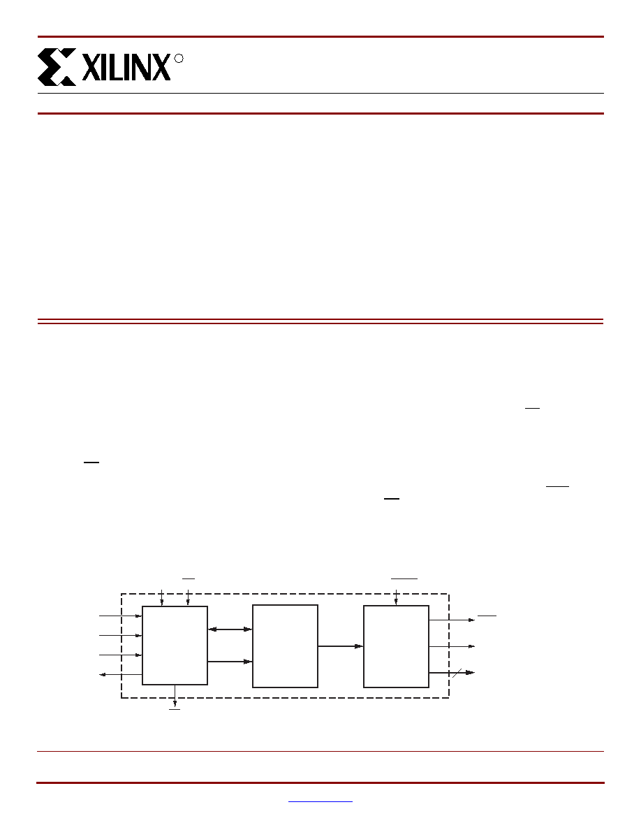
X-Ref Target - Figure 1
Figure 1: XC18V00 Series Block Diagram
Control
and
JTAG
Interface
Memory
Serial
or
Parallel
Interface
D0 DATA
Serial or Parallel Mode
D[1:7]
Parallel Interface
Data
Address
CLK
CE
TCK
TMS
TDI
TDO
OE/RESET
CEO
Data
DS026_01_040204
7
CF
相关PDF资料 |
PDF描述 |
|---|---|
| RPR40-11005S-B | CONV DC/DC 40W 40-160VIN 05VOUT |
| LTC4252-2CMS#TRPBF | IC CNTRLR HOTSWAP NEGVOLT 10MSOP |
| AT17LV010A-10JC | IC CONFIG SEEPROM 1M 3.3V 20PLCC |
| T97R108K6R3CAB | CAP TANT 1000UF 6.3V 10% 3024 |
| V72C5H100B | CONVERTER MOD DC/DC 5V 100W |
相关代理商/技术参数 |
参数描述 |
|---|---|
| XC18V02VQG44C0262 | 制造商:Xilinx 功能描述: |
| XC18V02VQG44C0936 | 制造商:Xilinx 功能描述:IC,Configuration Memory |
| XC18V04PC20 | 制造商:XILINX 制造商全称:XILINX 功能描述:In-System Programmable Configuration PROMs |
| XC18V04PC20C | 制造商:XILINX 制造商全称:XILINX 功能描述:In-System Programmable Configuration PROMs |
| XC18V04PC44 | 制造商:XILINX 制造商全称:XILINX 功能描述:In-System Programmable Configuration PROMs |
发布紧急采购,3分钟左右您将得到回复。