参数资料
| 型号: | XC2S15-5VQ100I |
| 厂商: | Xilinx Inc |
| 文件页数: | 16/99页 |
| 文件大小: | 0K |
| 描述: | IC FPGA 2.5V I-TEMP 100-VQFP |
| 标准包装: | 90 |
| 系列: | Spartan®-II |
| LAB/CLB数: | 96 |
| 逻辑元件/单元数: | 432 |
| RAM 位总计: | 16384 |
| 输入/输出数: | 60 |
| 门数: | 15000 |
| 电源电压: | 2.375 V ~ 2.625 V |
| 安装类型: | 表面贴装 |
| 工作温度: | -40°C ~ 100°C |
| 封装/外壳: | 100-TQFP |
| 供应商设备封装: | 100-VQFP(14x14) |
第1页第2页第3页第4页第5页第6页第7页第8页第9页第10页第11页第12页第13页第14页第15页当前第16页第17页第18页第19页第20页第21页第22页第23页第24页第25页第26页第27页第28页第29页第30页第31页第32页第33页第34页第35页第36页第37页第38页第39页第40页第41页第42页第43页第44页第45页第46页第47页第48页第49页第50页第51页第52页第53页第54页第55页第56页第57页第58页第59页第60页第61页第62页第63页第64页第65页第66页第67页第68页第69页第70页第71页第72页第73页第74页第75页第76页第77页第78页第79页第80页第81页第82页第83页第84页第85页第86页第87页第88页第89页第90页第91页第92页第93页第94页第95页第96页第97页第98页第99页

Spartan-II FPGA Family: Functional Description
DS001-2 (v2.8) June 13, 2008
Module 2 of 4
Product Specification
23
R
Master Serial Mode
In Master Serial mode, the CCLK output of the FPGA drives
a Xilinx PROM which feeds a serial stream of configuration
data to the FPGA’s DIN input. Figure 15 shows a Master
Serial FPGA configuring a Slave Serial FPGA from a
PROM. A Spartan-II device in Master Serial mode should
be connected as shown for the device on the left side.
Master Serial mode is selected by a <00x> on the mode
pins (M0, M1, M2). The PROM RESET pin is driven by INIT,
and CE input is driven by DONE. The interface is identical
to the slave serial mode except that an oscillator internal to
the FPGA is used to generate the configuration clock
(CCLK). Any of a number of different frequencies ranging
from 4 to 60 MHz can be set using the ConfigRate option in
the Xilinx software. On power-up, while the first 60 bytes of
the configuration data are being loaded, the CCLK
frequency is always 2.5 MHz. This frequency is used until
the ConfigRate bits, part of the configuration file, have been
loaded into the FPGA, at which point, the frequency
changes to the selected ConfigRate. Unless a different
frequency is specified in the design, the default ConfigRate
is 4 MHz. The frequency of the CCLK signal created by the
internal oscillator has a variance of +45%, –30% from the
specified value.
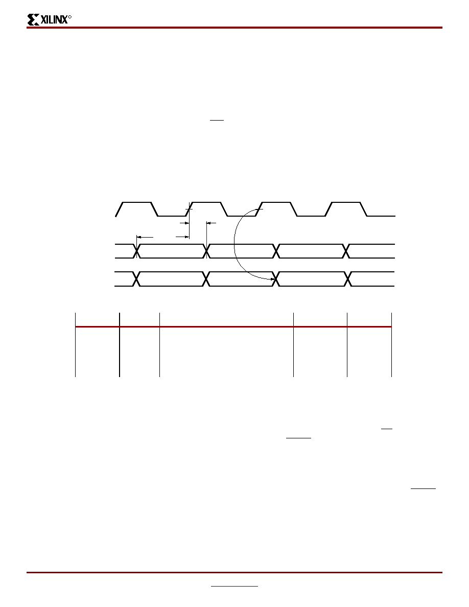
Figure 17 shows the timing for Master Serial configuration.
The FPGA accepts one bit of configuration data on each
rising CCLK edge. After the FPGA has been loaded, the
data for the next device in a daisy-chain is presented on the
DOUT pin after the rising CCLK edge.
Slave Parallel Mode
The Slave Parallel mode is the fastest configuration option.
Byte-wide data is written into the FPGA. A BUSY flag is
provided for controlling the flow of data at a clock frequency
FCCNH above 50 MHz.
Figure 18, page 24 shows the connections for two
Spartan-II devices using the Slave Parallel mode. Slave
Parallel mode is selected by a <011> on the mode pins (M0,
M1, M2).
If a configuration file of the format .bit, .rbt, or non-swapped
HEX is used for parallel programming, then the most
significant bit (i.e. the left-most bit of each configuration
byte, as displayed in a text editor) must be routed to the D0
input on the FPGA.
The agent controlling configuration is not shown. Typically,
a processor, a microcontroller, or CPLD controls the Slave
Parallel interface. The controlling agent provides byte-wide
configuration data, CCLK, a Chip Select (CS) signal and a
Write signal (WRITE). If BUSY is asserted (High) by the
FPGA, the data must be held until BUSY goes Low.
After configuration, the pins of the Slave Parallel port
(D0-D7) can be used as additional user I/O. Alternatively,
the port may be retained to permit high-speed 8-bit
readback. Then data can be read by de-asserting WRITE.
Figure 17: Master Serial Mode Timing
Serial Data In
CCLK
(Output)
Serial DOUT
(Output)
TDSCK
TCCO
TCKDS
DS001_17_110101
.
Symbol
Description
Units
TDSCK
CCLK
DIN setup
5.0
ns, min
TCKDS
DIN hold
0.0
ns, min
Frequency tolerance with respect to
nominal
+45%, –30%
-
相关PDF资料 |
PDF描述 |
|---|---|
| XC3S50A-5VQG100C | IC FPGA SPARTAN-3A 50K 100-VQFP |
| AMM28DRYI | CONN EDGECARD 56POS DIP .156 SLD |
| EMC65DRTN-S93 | CONN EDGECARD 130PS DIP .100 SLD |
| EMC65DRTH-S93 | CONN EDGECARD 130PS DIP .100 SLD |
| HMC44DRYI-S13 | CONN EDGECARD 88POS .100 EXTEND |
相关代理商/技术参数 |
参数描述 |
|---|---|
| XC2S15-5VQG100C | 功能描述:IC SPARTAN-II FPGA 15K 100-VQFP RoHS:是 类别:集成电路 (IC) >> 嵌入式 - FPGA(现场可编程门阵列) 系列:Spartan®-II 标准包装:24 系列:ECP2 LAB/CLB数:1500 逻辑元件/单元数:12000 RAM 位总计:226304 输入/输出数:131 门数:- 电源电压:1.14 V ~ 1.26 V 安装类型:表面贴装 工作温度:0°C ~ 85°C 封装/外壳:208-BFQFP 供应商设备封装:208-PQFP(28x28) |
| XC2S15-5VQG100I | 制造商:Xilinx 功能描述:FPGA SPARTAN-II 15K GATES 432 CELLS 263MHZ 2.5V 100VTQFP - Trays 制造商:Xilinx 功能描述:IC SYSTEM GATE |
| XC2S15-6CS144C | 功能描述:IC FPGA 2.5V C-TEMP 144-CSBGA RoHS:否 类别:集成电路 (IC) >> 嵌入式 - FPGA(现场可编程门阵列) 系列:Spartan®-II 产品变化通告:XC4000(E,L) Discontinuation 01/April/2002 标准包装:24 系列:XC4000E/X LAB/CLB数:100 逻辑元件/单元数:238 RAM 位总计:3200 输入/输出数:80 门数:3000 电源电压:4.5 V ~ 5.5 V 安装类型:表面贴装 工作温度:-40°C ~ 100°C 封装/外壳:120-BCBGA 供应商设备封装:120-CPGA(34.55x34.55) |
| XC2S15-6CS144I | 制造商:XILINX 制造商全称:XILINX 功能描述:Spartan-II FPGA Family |
| XC2S15-6CSG144C | 制造商:XILINX 制造商全称:XILINX 功能描述:Spartan-II FPGA Family |
发布紧急采购,3分钟左右您将得到回复。