参数资料
| 型号: | XC2S30-5TQG144I |
| 厂商: | Xilinx Inc |
| 文件页数: | 4/99页 |
| 文件大小: | 0K |
| 描述: | IC FPGA 2.5V I-TEMP 144-TQFP |
| 标准包装: | 60 |
| 系列: | Spartan®-II |
| LAB/CLB数: | 216 |
| 逻辑元件/单元数: | 972 |
| RAM 位总计: | 24576 |
| 输入/输出数: | 92 |
| 门数: | 30000 |
| 电源电压: | 2.375 V ~ 2.625 V |
| 安装类型: | 表面贴装 |
| 工作温度: | -40°C ~ 100°C |
| 封装/外壳: | 144-LQFP |
| 供应商设备封装: | 144-TQFP(20x20) |
| 其它名称: | Q5852174 |
第1页第2页第3页当前第4页第5页第6页第7页第8页第9页第10页第11页第12页第13页第14页第15页第16页第17页第18页第19页第20页第21页第22页第23页第24页第25页第26页第27页第28页第29页第30页第31页第32页第33页第34页第35页第36页第37页第38页第39页第40页第41页第42页第43页第44页第45页第46页第47页第48页第49页第50页第51页第52页第53页第54页第55页第56页第57页第58页第59页第60页第61页第62页第63页第64页第65页第66页第67页第68页第69页第70页第71页第72页第73页第74页第75页第76页第77页第78页第79页第80页第81页第82页第83页第84页第85页第86页第87页第88页第89页第90页第91页第92页第93页第94页第95页第96页第97页第98页第99页
Spartan-II FPGA Family: Functional Description
DS001-2 (v2.8) June 13, 2008
Module 2 of 4
Product Specification
12
R
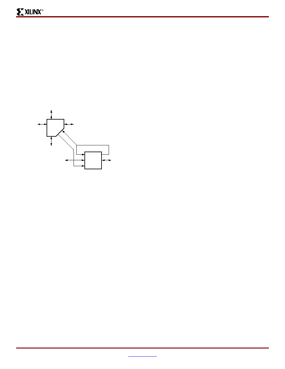
Local Routing
The local routing resources, as shown in Figure 6, provide
the following three types of connections:
Interconnections among the LUTs, flip-flops, and
General Routing Matrix (GRM)
Internal CLB feedback paths that provide high-speed
connections to LUTs within the same CLB, chaining
them together with minimal routing delay
Direct paths that provide high-speed connections
between horizontally adjacent CLBs, eliminating the
delay of the GRM
General Purpose Routing
Most Spartan-II FPGA signals are routed on the general
purpose routing, and consequently, the majority of
interconnect resources are associated with this level of the
routing hierarchy. The general routing resources are
located in horizontal and vertical routing channels
associated with the rows and columns CLBs. The
general-purpose routing resources are listed below.
Adjacent to each CLB is a General Routing Matrix
(GRM). The GRM is the switch matrix through which
horizontal and vertical routing resources connect, and
is also the means by which the CLB gains access to
the general purpose routing.
24 single-length lines route GRM signals to adjacent
GRMs in each of the four directions.
96 buffered Hex lines route GRM signals to other
GRMs six blocks away in each one of the four
directions. Organized in a staggered pattern, Hex lines
may be driven only at their endpoints. Hex-line signals
can be accessed either at the endpoints or at the
midpoint (three blocks from the source). One third of
the Hex lines are bidirectional, while the remaining
ones are unidirectional.
12 Longlines are buffered, bidirectional wires that
distribute signals across the device quickly and
efficiently. Vertical Longlines span the full height of the
device, and horizontal ones span the full width of the
device.
I/O Routing
Spartan-II devices have additional routing resources
around their periphery that form an interface between the
CLB array and the IOBs. This additional routing, called the
VersaRing, facilitates pin-swapping and pin-locking, such
that logic redesigns can adapt to existing PCB layouts.
Time-to-market is reduced, since PCBs and other system
components can be manufactured while the logic design is
still in progress.
Dedicated Routing
Some classes of signal require dedicated routing resources
to maximize performance. In the Spartan-II architecture,
dedicated routing resources are provided for two classes of
signal.
Horizontal routing resources are provided for on-chip
3-state busses. Four partitionable bus lines are
provided per CLB row, permitting multiple busses
within a row, as shown in Figure 7.
Two dedicated nets per CLB propagate carry signals
vertically to the adjacent CLB.
Global Routing
Global Routing resources distribute clocks and other
signals with very high fanout throughout the device.
Spartan-II devices include two tiers of global routing
resources referred to as primary and secondary global
routing resources.
The
primary
global
routing
resources
are
four
dedicated global nets with dedicated input pins that are
designed to distribute high-fanout clock signals with
minimal skew. Each global clock net can drive all CLB,
IOB, and block RAM clock pins. The primary global
nets may only be driven by global buffers. There are
four global buffers, one for each global net.
The secondary global routing resources consist of 24
backbone lines, 12 across the top of the chip and 12
across bottom. From these lines, up to 12 unique
signals per column can be distributed via the 12
longlines in the column. These secondary resources
are more flexible than the primary resources since they
are not restricted to routing only to clock pins.
Figure 6: Spartan-II Local Routing
DS001_06_032300
CLB
GRM
To
Adjacent
GRM
To Adjacent
GRM
Direct
Connection
To Adjacent
CLB
To Adjacent
GRM
To Adjacent
GRM
Direct Connection
To Adjacent
CLB
相关PDF资料 |
PDF描述 |
|---|---|
| XC2S30-6TQ144C | IC FPGA 2.5V C-TEMP 144-TQFP |
| 24LC024HT-E/MS | IC EEPROM 2KBIT 400KHZ 8MSOP |
| 748610-2 | CONT, HD22 CS SCKT, 30AU |
| 24LC014T-E/MS | IC EEPROM 1KBIT 400KHZ 8MSOP |
| XC2S30-5TQ144I | IC FPGA 2.5V I-TEMP 144-TQFP |
相关代理商/技术参数 |
参数描述 |
|---|---|
| XC2S30-5VQ100C | 功能描述:IC FPGA 2.5V 216 CLB'S 100-VQFP RoHS:否 类别:集成电路 (IC) >> 嵌入式 - FPGA(现场可编程门阵列) 系列:Spartan®-II 标准包装:40 系列:Spartan® 6 LX LAB/CLB数:3411 逻辑元件/单元数:43661 RAM 位总计:2138112 输入/输出数:358 门数:- 电源电压:1.14 V ~ 1.26 V 安装类型:表面贴装 工作温度:-40°C ~ 100°C 封装/外壳:676-BGA 供应商设备封装:676-FBGA(27x27) |
| XC2S30-5VQ100I | 功能描述:IC FPGA 2.5V I-TEMP 100-VQFP RoHS:否 类别:集成电路 (IC) >> 嵌入式 - FPGA(现场可编程门阵列) 系列:Spartan®-II 标准包装:40 系列:Spartan® 6 LX LAB/CLB数:3411 逻辑元件/单元数:43661 RAM 位总计:2138112 输入/输出数:358 门数:- 电源电压:1.14 V ~ 1.26 V 安装类型:表面贴装 工作温度:-40°C ~ 100°C 封装/外壳:676-BGA 供应商设备封装:676-FBGA(27x27) |
| XC2S30-5VQG100C | 功能描述:IC FPGA 2.5V 216 CLB'S 100-VQFP RoHS:是 类别:集成电路 (IC) >> 嵌入式 - FPGA(现场可编程门阵列) 系列:Spartan®-II 标准包装:60 系列:XP LAB/CLB数:- 逻辑元件/单元数:10000 RAM 位总计:221184 输入/输出数:244 门数:- 电源电压:1.71 V ~ 3.465 V 安装类型:表面贴装 工作温度:0°C ~ 85°C 封装/外壳:388-BBGA 供应商设备封装:388-FPBGA(23x23) 其它名称:220-1241 |
| XC2S30-5VQG100I | 制造商:Xilinx 功能描述:FPGA SPARTAN-II 30K GATES 972 CELLS 263MHZ 2.5V 100VTQFP - Trays 制造商:Xilinx 功能描述:IC SYSTEM GATE |
| XC2S30-6CS144C | 功能描述:IC FPGA 2.5V C-TEMP 144-CSBGA RoHS:否 类别:集成电路 (IC) >> 嵌入式 - FPGA(现场可编程门阵列) 系列:Spartan®-II 标准包装:40 系列:Spartan® 6 LX LAB/CLB数:3411 逻辑元件/单元数:43661 RAM 位总计:2138112 输入/输出数:358 门数:- 电源电压:1.14 V ~ 1.26 V 安装类型:表面贴装 工作温度:-40°C ~ 100°C 封装/外壳:676-BGA 供应商设备封装:676-FBGA(27x27) |
发布紧急采购,3分钟左右您将得到回复。