参数资料
| 型号: | XC2V4000-5BF957C |
| 厂商: | Xilinx Inc |
| 文件页数: | 235/318页 |
| 文件大小: | 0K |
| 描述: | IC FPGA VIRTEX II 3M 957-FCBGA |
| 产品变化通告: | FPGA Family Discontinuation 18/Apr/2011 |
| 标准包装: | 1 |
| 系列: | Virtex®-II |
| LAB/CLB数: | 5760 |
| RAM 位总计: | 2211840 |
| 输入/输出数: | 684 |
| 门数: | 4000000 |
| 电源电压: | 1.425 V ~ 1.575 V |
| 安装类型: | 表面贴装 |
| 工作温度: | 0°C ~ 85°C |
| 封装/外壳: | 957-BBGA,FCBGA |
| 供应商设备封装: | 957-FCBGA(40x40) |
第1页第2页第3页第4页第5页第6页第7页第8页第9页第10页第11页第12页第13页第14页第15页第16页第17页第18页第19页第20页第21页第22页第23页第24页第25页第26页第27页第28页第29页第30页第31页第32页第33页第34页第35页第36页第37页第38页第39页第40页第41页第42页第43页第44页第45页第46页第47页第48页第49页第50页第51页第52页第53页第54页第55页第56页第57页第58页第59页第60页第61页第62页第63页第64页第65页第66页第67页第68页第69页第70页第71页第72页第73页第74页第75页第76页第77页第78页第79页第80页第81页第82页第83页第84页第85页第86页第87页第88页第89页第90页第91页第92页第93页第94页第95页第96页第97页第98页第99页第100页第101页第102页第103页第104页第105页第106页第107页第108页第109页第110页第111页第112页第113页第114页第115页第116页第117页第118页第119页第120页第121页第122页第123页第124页第125页第126页第127页第128页第129页第130页第131页第132页第133页第134页第135页第136页第137页第138页第139页第140页第141页第142页第143页第144页第145页第146页第147页第148页第149页第150页第151页第152页第153页第154页第155页第156页第157页第158页第159页第160页第161页第162页第163页第164页第165页第166页第167页第168页第169页第170页第171页第172页第173页第174页第175页第176页第177页第178页第179页第180页第181页第182页第183页第184页第185页第186页第187页第188页第189页第190页第191页第192页第193页第194页第195页第196页第197页第198页第199页第200页第201页第202页第203页第204页第205页第206页第207页第208页第209页第210页第211页第212页第213页第214页第215页第216页第217页第218页第219页第220页第221页第222页第223页第224页第225页第226页第227页第228页第229页第230页第231页第232页第233页第234页当前第235页第236页第237页第238页第239页第240页第241页第242页第243页第244页第245页第246页第247页第248页第249页第250页第251页第252页第253页第254页第255页第256页第257页第258页第259页第260页第261页第262页第263页第264页第265页第266页第267页第268页第269页第270页第271页第272页第273页第274页第275页第276页第277页第278页第279页第280页第281页第282页第283页第284页第285页第286页第287页第288页第289页第290页第291页第292页第293页第294页第295页第296页第297页第298页第299页第300页第301页第302页第303页第304页第305页第306页第307页第308页第309页第310页第311页第312页第313页第314页第315页第316页第317页第318页
Virtex-II Platform FPGAs: Functional Description
R
DS031-2 (v3.5) November 5, 2007
Module 2 of 4
Product Specification
23
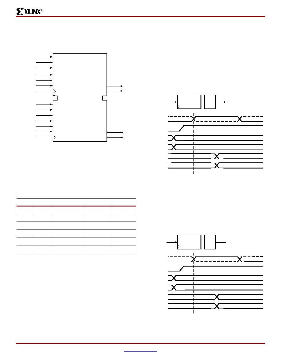
Each block SelectRAM cell is a fully synchronous memory,
as illustrated in Figure 30. The two ports have independent
inputs and outputs and are independently clocked.
Port Aspect Ratios
Table 16 shows the depth and the width aspect ratios for the
18 Kbit block SelectRAM. Virtex-II block SelectRAM also
includes dedicated routing resources to provide an efficient
interface with CLBs, block SelectRAM, and multipliers.
Read/Write Operations
The Virtex-II block SelectRAM read operation is fully syn-
chronous. An address is presented, and the read operation
is enabled by control signals WEA and WEB in addition to
ENA or ENB. Then, depending on clock polarity, a rising or
falling clock edge causes the stored data to be loaded into
output registers.
The write operation is also fully synchronous. Data and
address are presented, and the write operation is enabled
by control signals WEA or WEB in addition to ENA or ENB.
Then, again depending on the clock input mode, a rising or
falling clock edge causes the data to be loaded into the
memory cell addressed.
A write operation performs a simultaneous read operation.
Three different options are available, selected by configura-
tion:
1.
“WRITE_FIRST”
The “WRITE_FIRST” option is a transparent mode. The
same clock edge that writes the data input (DI) into the
memory also transfers DI into the output registers DO
as shown in Figure 31.
2.
“READ_FIRST”
The “READ_FIRST” option is a read-before-write mode.
The same clock edge that writes data input (DI) into the
memory also transfers the prior content of the memory
cell addressed into the data output registers DO, as
shown in Figure 32.
Figure 30: 18 Kbit Block SelectRAM in Dual-Port Mode
Table 16: 18 Kbit Block SelectRAM Port Aspect Ratio
Width
Depth
Address Bus
Data Bus
Parity Bus
1
16,384
ADDR[13:0]
DATA[0]
N/A
2
8,192
ADDR[12:0]
DATA[1:0]
N/A
4
4,096
ADDR[11:0]
DATA[3:0]
N/A
9
2,048
ADDR[10:0]
DATA[7:0]
Parity[0]
18
1,024
ADDR[9:0]
DATA[15:0]
Parity[1:0]
36
512
ADDR[8:0]
DATA[31:0]
Parity[3:0]
DOPA
DOPB
DIPA
ADDRA
WEA
ENA
SSRA
CLKA
DIPB
ADDRB
WEB
ENB
SSRB
CLKB
18 Kbit Block SelectRAM
DS031_11_071602
DOB
DOA
DIA
DIB
Figure 31: WRITE_FIRST Mode
Figure 32: READ_FIRST Mode
CLK
WE
Data_in
New
aa
Address
Internal
Memory
DO
Data_out = Data_in
Data_out
DI
DS031_14_102000
New
RAM Contents
New
Old
CLK
WE
Data_in
New
aa
Old
Address
Internal
Memory
DO
Prior stored data
Data_out
DI
DS031_13_102000
RAM Contents
New
Old
相关PDF资料 |
PDF描述 |
|---|---|
| AMC44DRTN | CONN EDGECARD 88POS .100 DIP SLD |
| AMC44DRTH | CONN EDGECARD 88POS .100 DIP SLD |
| AMC44DREN | CONN EDGECARD 88POS .100 EYELET |
| AMC44DREH | CONN EDGECARD 88POS .100 EYELET |
| ACB108DHRN | CONN CARD EXTEND 216POS .050" |
相关代理商/技术参数 |
参数描述 |
|---|---|
| XC2V4000-5BF957I | 功能描述:IC FPGA VIRTEX-II 957FCBGA RoHS:否 类别:集成电路 (IC) >> 嵌入式 - FPGA(现场可编程门阵列) 系列:Virtex®-II 产品变化通告:XC4000(E,L) Discontinuation 01/April/2002 标准包装:24 系列:XC4000E/X LAB/CLB数:100 逻辑元件/单元数:238 RAM 位总计:3200 输入/输出数:80 门数:3000 电源电压:4.5 V ~ 5.5 V 安装类型:表面贴装 工作温度:-40°C ~ 100°C 封装/外壳:120-BCBGA 供应商设备封装:120-CPGA(34.55x34.55) |
| XC2V4000-5BFG957C | 制造商:Xilinx 功能描述:FPGA VIRTEX-II 4M GATES 51840 CELLS 750MHZ 0.15UM/0.12UM 1.5 - Trays |
| XC2V4000-5BFG957I | 功能描述:IC FPGA VIRTEX-II 957FCBGA RoHS:否 类别:集成电路 (IC) >> 嵌入式 - FPGA(现场可编程门阵列) 系列:Virtex®-II 产品变化通告:XC4000(E,L) Discontinuation 01/April/2002 标准包装:24 系列:XC4000E/X LAB/CLB数:100 逻辑元件/单元数:238 RAM 位总计:3200 输入/输出数:80 门数:3000 电源电压:4.5 V ~ 5.5 V 安装类型:表面贴装 工作温度:-40°C ~ 100°C 封装/外壳:120-BCBGA 供应商设备封装:120-CPGA(34.55x34.55) |
| XC2V4000-5CS144C | 制造商:XILINX 制造商全称:XILINX 功能描述:Virtex-II Platform FPGAs: Complete Data Sheet |
| XC2V4000-5CS144I | 制造商:XILINX 制造商全称:XILINX 功能描述:Virtex-II Platform FPGAs: Complete Data Sheet |
发布紧急采购,3分钟左右您将得到回复。