参数资料
| 型号: | XC3042L-8VQ100C |
| 厂商: | Xilinx Inc |
| 文件页数: | 67/76页 |
| 文件大小: | 0K |
| 描述: | IC FPGA 3.3V C-TEMP 100-VQFP |
| 产品变化通告: | XC3000(L) Discontinuation 01/Feb/2003 |
| 标准包装: | 450 |
| 系列: | XC3000A/L |
| LAB/CLB数: | 144 |
| RAM 位总计: | 30784 |
| 输入/输出数: | 82 |
| 门数: | 3000 |
| 电源电压: | 3 V ~ 3.6 V |
| 安装类型: | 表面贴装 |
| 工作温度: | 0°C ~ 85°C |
| 封装/外壳: | 100-TQFP |
| 供应商设备封装: | 100-VQFP(14x14) |
第1页第2页第3页第4页第5页第6页第7页第8页第9页第10页第11页第12页第13页第14页第15页第16页第17页第18页第19页第20页第21页第22页第23页第24页第25页第26页第27页第28页第29页第30页第31页第32页第33页第34页第35页第36页第37页第38页第39页第40页第41页第42页第43页第44页第45页第46页第47页第48页第49页第50页第51页第52页第53页第54页第55页第56页第57页第58页第59页第60页第61页第62页第63页第64页第65页第66页当前第67页第68页第69页第70页第71页第72页第73页第74页第75页第76页
R
November 9, 1998 (Version 3.1)
7-9
XC3000 Series Field Programmable Gate Arrays
7
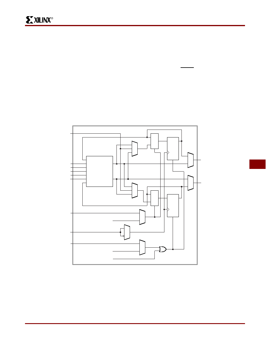
Configurable Logic Block
The array of CLBs provides the functional elements from
which the user’s logic is constructed. The logic blocks are
arranged in a matrix within the perimeter of IOBs. For
example, the XC3020A has 64 such blocks arranged in 8
rows and 8 columns. The development system is used to
compile the configuration data which is to be loaded into
the internal configuration memory to define the operation
and interconnection of each block. User definition of CLBs
and their interconnecting networks may be done by auto-
matic translation from a schematic-capture logic diagram or
optionally by installing library or user macros.
Each CLB has a combinatorial logic section, two flip-flops,
and an internal control section. See Figure 5. There are:
five logic inputs (A, B, C, D and E); a common clock input
(K); an asynchronous direct RESET input (RD); and an
enable clock (EC). All may be driven from the interconnect
resources adjacent to the blocks. Each CLB also has two
outputs (X and Y) which may drive interconnect networks.
Data input for either flip-flop within a CLB is supplied from
the function F or G outputs of the combinatorial logic, or the
block input, DI. Both flip-flops in each CLB share the asyn-
chronous RD which, when enabled and High, is dominant
over clocked inputs. All flip-flops are reset by the
active-Low chip input, RESET, or during the configuration
process. The flip-flops share the enable clock (EC) which,
when Low, recirculates the flip-flops’ present states and
inhibits response to the data-in or combinatorial function
inputs on a CLB. The user may enable these control inputs
and select their sources. The user may also select the
clock net input (K), as well as its active sense within each
CLB. This programmable inversion eliminates the need to
route both phases of a clock signal throughout the device.
Q
COMBINATORIAL
FUNCTION
LOGIC
VARIABLES
D
RD
G
F
DIN
F
G
QX
QY
DIN
F
G
QY
QX
F
Q
D
RD
ENABLE CLOCK
CLOCK
DIRECT
RESET
1 (ENABLE)
A
B
C
D
E
DI
EC
K
RD
Y
X
X3032
0 (INHIBIT)
(GLOBAL RESET)
CLB OUTPUTS
DATA IN
0
1
0
1
MUX
Figure 5: Configurable Logic Block.
Each CLB includes a combinatorial logic section, two flip-flops and a program memory controlled multiplexer selection of
function. It has the following:
-
five logic variable inputs A, B, C, D, and E
-
a direct data in DI
-
an enable clock EC
-
a clock (invertible) K
-
an asynchronous direct RESET RD
-
two outputs X and Y
Product Obsolete or Under Obsolescence
相关PDF资料 |
PDF描述 |
|---|---|
| ABB66DHAN-S621 | CONN EDGECARD 132PS R/A .050 SLD |
| ABB66DHAD-S621 | CONN EDGECARD 132PS R/A .050 SLD |
| ASM43DTAI | CONN EDGECARD 86POS R/A .156 SLD |
| XC3030L-8VQ64I | IC FPGA I-TEMP 3.3V 64-VQFP |
| ASM43DTMI | CONN EDGECARD 86POS R/A .156 SLD |
相关代理商/技术参数 |
参数描述 |
|---|---|
| XC3042L-8VQ100I | 功能描述:IC FPGA 3.3V I-TEMP 100-VQFP RoHS:否 类别:集成电路 (IC) >> 嵌入式 - FPGA(现场可编程门阵列) 系列:XC3000A/L 产品变化通告:XC4000(E,L) Discontinuation 01/April/2002 标准包装:24 系列:XC4000E/X LAB/CLB数:100 逻辑元件/单元数:238 RAM 位总计:3200 输入/输出数:80 门数:3000 电源电压:4.5 V ~ 5.5 V 安装类型:表面贴装 工作温度:-40°C ~ 100°C 封装/外壳:120-BCBGA 供应商设备封装:120-CPGA(34.55x34.55) |
| XC3042PC84BS70C | 制造商:Xilinx 功能描述: |
| XC3042PQ100BKJ9721 | 制造商:XI 功能描述:3042PQ100BK XILINX S9I7B |
| XC3064 | 制造商:XILINX 制造商全称:XILINX 功能描述:Logic Cell Array Families |
| XC3064100PC84C | 制造商:XILINX 功能描述:NEW |
发布紧急采购,3分钟左右您将得到回复。