参数资料
| 型号: | XC3130A-3PQ100C |
| 厂商: | Xilinx Inc |
| 文件页数: | 11/76页 |
| 文件大小: | 0K |
| 描述: | IC LOGIC CL ARRAY 3000GAT 100PQF |
| 产品变化通告: | XC4000XL/E, XC9500XV, XC3100A Discontinuance 12/Apr/2010 |
| 标准包装: | 66 |
| 系列: | XC3000A/L |
| LAB/CLB数: | 100 |
| RAM 位总计: | 22176 |
| 输入/输出数: | 80 |
| 门数: | 2000 |
| 电源电压: | 4.25 V ~ 5.25 V |
| 安装类型: | 表面贴装 |
| 工作温度: | 0°C ~ 85°C |
| 封装/外壳: | 100-BQFP |
| 供应商设备封装: | 100-QFP(14x20) |
| 其它名称: | 122-1041 |
第1页第2页第3页第4页第5页第6页第7页第8页第9页第10页当前第11页第12页第13页第14页第15页第16页第17页第18页第19页第20页第21页第22页第23页第24页第25页第26页第27页第28页第29页第30页第31页第32页第33页第34页第35页第36页第37页第38页第39页第40页第41页第42页第43页第44页第45页第46页第47页第48页第49页第50页第51页第52页第53页第54页第55页第56页第57页第58页第59页第60页第61页第62页第63页第64页第65页第66页第67页第68页第69页第70页第71页第72页第73页第74页第75页第76页
R
November 9, 1998 (Version 3.1)
7-21
XC3000 Series Field Programmable Gate Arrays
7
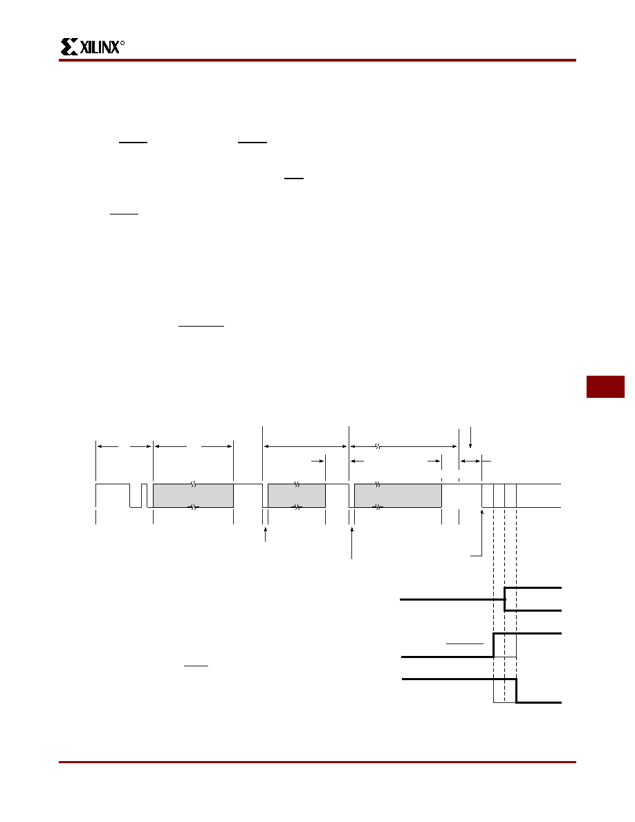
a synchronous start-up sequence and become operational.
See Figure 22. Two CCLK cycles after the completion of
loading configuration data, the user I/O pins are enabled as
configured. As selected, the internal user-logic RESET is
released either one clock cycle before or after the I/O pins
become active. A similar timing selection is programmable
for the DONE/PROG output signal. DONE/PROG may also
be programmed to be an open drain or include a pull-up
resistor to accommodate wired ANDing. The High During
Configuration (HDC) and Low During Configuration (LDC)
are two user I/O pins which are driven active while an
FPGA is in its Initialization, Clear or Configure states. They
and DONE/PROG provide signals for control of external
logic signals such as RESET, bus enable or PROM enable
during configuration. For parallel Master configuration
modes, these signals provide PROM enable control and
allow the data pins to be shared with user logic signals.
User I/O inputs can be programmed to be either TTL or
CMOS compatible thresholds. At power-up, all inputs have
TTL thresholds and can change to CMOS thresholds at the
completion of configuration if the user has selected CMOS
thresholds. The threshold of PWRDWN and the direct clock
inputs are fixed at a CMOS level.
If the crystal oscillator is used, it will begin operation before
configuration is complete to allow time for stabilization
before it is connected to the internal circuitry.
Configuration Data
Configuration data to define the function and interconnec-
tion within a Field Programmable Gate Array is loaded from
an external storage at power-up and after a re-program sig-
nal. Several methods of automatic and controlled loading of
the required data are available. Logic levels applied to
mode selection pins at the start of configuration time deter-
mine the method to be used. See Table 1. The data may be
either bit-serial or byte-parallel, depending on the configu-
ration mode. The different FPGAs have different sizes and
numbers of data frames. To maintain compatibility between
various device types, the Xilinx product families use com-
patible configuration formats. For the XC3020A, configura-
tion requires 14779 bits for each device, arranged in 197
data frames. An additional 40 bits are used in the header.
See Figure 22. The specific data format for each device is
produced by the development system and one or more of
these files can then be combined and appended to a length
count preamble and be transformed into a PROM format
file by the development system. A compatibility exception
precludes the use of an XC2000-series device as the mas-
ter for XC3000-series devices if their DONE or RESET are
programmed to occur after their outputs become active.
The Tie Option defines output levels of unused blocks of a
design and connects these to unused routing resources.
This prevents indeterminate levels that might produce par-
asitic supply currents. If unused blocks are not sufficient to
complete the tie, the user can indicate nets which must not
Preamble
Length Count
Data
12
24
4
Data Frame
Start
Bit
Start
Bit
3
4
Last Frame
Postamble
I/O Active
DONE
Internal Reset
Length Count*
The configuration data consists of a composite
40-bit preamble/length count, followed by one or
more concatenated FPGA programs, separated by
4-bit postambles. An additional final postamble bit
is added for each slave device and the result rounded
up to a byte boundary. The length count is two less
than the number of resulting bits.
Timing of the assertion of DONE and
termination of the INTERNAL RESET
may each be programmed to occur
one cycle before or after the I/O outputs
become active.
Heavy lines indicate the default condition
X5988
PROGRAM
Weak Pull-Up
*
Stop
3
STOP
DIN
Figure 22: Configuration and Start-up of One or More FPGAs.
Product Obsolete or Under Obsolescence
相关PDF资料 |
PDF描述 |
|---|---|
| XC3130A-3PC84C | IC LOGIC CL ARRAY 3000GAT 84PLCC |
| RCB108DHBR | CONN EDGECARD 216PS R/A .050 DIP |
| XC3120A-3PC68C | IC LOGIC CL ARRAY 2000GAT 68PLCC |
| ASC49DRYN-S93 | CONN EDGECARD 98POS DIP .100 SLD |
| XC3090A-7PC84C | IC LOGIC CL ARRAY 9000GAT 84PLCC |
相关代理商/技术参数 |
参数描述 |
|---|---|
| XC3130A-3PQ100C0262 | 制造商:Xilinx 功能描述: |
| XC3130A-3PQ100I | 制造商:Xilinx 功能描述: |
| XC3130A-3VQ100C | 制造商:Xilinx 功能描述: |
| XC3130A-3VQ100I | 制造商:XILINX 制造商全称:XILINX 功能描述:Field Programmable Gate Arrays (XC3000A/L, XC3100A/L) |
| XC3130A-3VQ64C | 制造商:XILINX 制造商全称:XILINX 功能描述:Field Programmable Gate Arrays (XC3000A/L, XC3100A/L) |
发布紧急采购,3分钟左右您将得到回复。