参数资料
| 型号: | XC3S1600E-5FGG320C |
| 厂商: | Xilinx Inc |
| 文件页数: | 218/227页 |
| 文件大小: | 0K |
| 描述: | IC FPGA SPARTAN-3E 1600K 320FBGA |
| 标准包装: | 84 |
| 系列: | Spartan®-3E |
| LAB/CLB数: | 3688 |
| 逻辑元件/单元数: | 33192 |
| RAM 位总计: | 663552 |
| 输入/输出数: | 250 |
| 门数: | 1600000 |
| 电源电压: | 1.14 V ~ 1.26 V |
| 安装类型: | 表面贴装 |
| 工作温度: | 0°C ~ 85°C |
| 封装/外壳: | 320-BGA |
| 供应商设备封装: | 320-FBGA(19x19) |
| 配用: | HW-XA3S1600E-UNI-G-ND - KIT DEVELOPMENT AUTOMOTIVE ECU |
第1页第2页第3页第4页第5页第6页第7页第8页第9页第10页第11页第12页第13页第14页第15页第16页第17页第18页第19页第20页第21页第22页第23页第24页第25页第26页第27页第28页第29页第30页第31页第32页第33页第34页第35页第36页第37页第38页第39页第40页第41页第42页第43页第44页第45页第46页第47页第48页第49页第50页第51页第52页第53页第54页第55页第56页第57页第58页第59页第60页第61页第62页第63页第64页第65页第66页第67页第68页第69页第70页第71页第72页第73页第74页第75页第76页第77页第78页第79页第80页第81页第82页第83页第84页第85页第86页第87页第88页第89页第90页第91页第92页第93页第94页第95页第96页第97页第98页第99页第100页第101页第102页第103页第104页第105页第106页第107页第108页第109页第110页第111页第112页第113页第114页第115页第116页第117页第118页第119页第120页第121页第122页第123页第124页第125页第126页第127页第128页第129页第130页第131页第132页第133页第134页第135页第136页第137页第138页第139页第140页第141页第142页第143页第144页第145页第146页第147页第148页第149页第150页第151页第152页第153页第154页第155页第156页第157页第158页第159页第160页第161页第162页第163页第164页第165页第166页第167页第168页第169页第170页第171页第172页第173页第174页第175页第176页第177页第178页第179页第180页第181页第182页第183页第184页第185页第186页第187页第188页第189页第190页第191页第192页第193页第194页第195页第196页第197页第198页第199页第200页第201页第202页第203页第204页第205页第206页第207页第208页第209页第210页第211页第212页第213页第214页第215页第216页第217页当前第218页第219页第220页第221页第222页第223页第224页第225页第226页第227页
Spartan-3E FPGA Family: Functional Description
DS312 (v4.1) July 19, 2013
Product Specification
90
support byte-wide data. However, after configuration, the
FPGA supports either x8 or x16 modes. In x16 mode, up to
eight additional user I/O pins are required for the upper data
bits, D[15:8].
Connecting a Spartan-3E FPGA to a x8/x16 Flash PROM is
simple, but does require a precaution. Various Flash PROM
vendors use slightly different interfaces to support both x8
and x16 modes. Some vendors (Intel, Micron, some
STMicroelectronics devices) use a straightforward interface
with pin naming that matches the FPGA connections.
However, the PROM’s A0 pin is wasted in x16 applications
and a separate FPGA user-I/O pin is required for the D15
data line. Fortunately, the FPGA A0 pin is still available as a
user I/O after configuration, even though it connects to the
Flash PROM.
Other vendors (AMD, Atmel, Silicon Storage Technology,
some STMicroelectronics devices) use a pin-efficient
interface but change the function of one pin, called
IO15/A-1, depending if the PROM is in x8 or x16 mode. In
x8 mode, BYTE# = 0, this pin is the least-significant
address line. The A0 address line selects the halfword
location. The A-1 address line selects the byte location.
When in x16 mode, BYTE# = 1, the IO15/A-1 pin becomes
the most-significant data bit, D15 because byte addressing
is not required in this mode. Check to see if the Flash
PROM has a pin named “IO15/A-1” or “DQ15/A-1”. If so, be
careful to connect x8/x16 Flash PROMs correctly, as shown
in Table 63. Also, remember that the D[14:8] data
connections require FPGA user I/O pins but that the D15
data is already connected for the FPGA’s A0 pin.
Some x8/x16 Flash PROMs have a long setup time
requirement on the BYTE# signal. For the FPGA to
configure correctly, the PROM must be in x8 mode with
BYTE# = 0 at power-on or when the FPGA’s PROG_B pin is
pulsed Low. If required, extend the BYTE# setup time for a
3.3V PROM using an external 680
Ω pull-down resistor on
the FPGA’s LDC2 pin or by delaying assertion of the CSI_B
select input to the FPGA.
Daisy-Chaining
If the application requires multiple FPGAs with different
configurations, then configure the FPGAs using a daisy
chain, as shown in Figure 59. Use BPI mode
(M[2:0] = <0:1:0> or <0:1:1>) for the FPGA connected to
the parallel NOR Flash PROM and Slave Parallel mode
(M[2:0] = <1:1:0>) for all downstream FPGAs in the
daisy-chain. If there are more than two FPGAs in the chain,
then last FPGA in the chain can be from any Xilinx FPGA
family. However, all intermediate FPGAs located in the
chain between the first and last FPGAs must from either the
Spartan-3E or Virtex-5 FPGA families.
After the master FPGA—the FPGA on the left in the
diagram—finishes loading its configuration data from the
parallel Flash PROM, the master device continues
generating addresses to the Flash PROM and asserts its
CSO_B output Low, enabling the next FPGA in the
daisy-chain. The next FPGA then receives parallel
configuration data from the Flash PROM. The master
FPGA’s CCLK output synchronizes data capture.
If HSWAP = 1, an external 4.7k
Ω pull-up resistor must be
added on the CSO_B pin. If HSWAP = 0, no external pull-up
is necessary.
Design Note
BPI mode daisy chain software support is available starting
in ISE 8.2i.
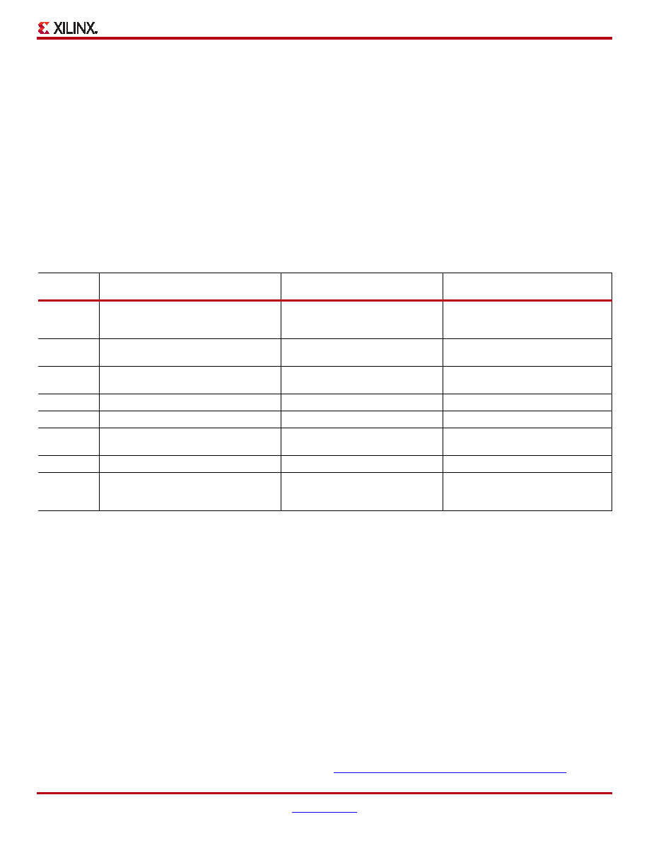
Table 63: FPGA Connections to Flash PROM with IO15/A-1 Pin
FPGA Pin
Connection to Flash PROM with
IO15/A-1 Pin
x8 Flash PROM Interface After
FPGA Configuration
x16 Flash PROM Interface After
FPGA Configuration
LDC2
BYTE#
Drive LDC2 Low or leave
unconnected and tie PROM BYTE#
input to GND
Drive LCD2 High
LDC1
OE#
Active-Low Flash PROM
output-enable control
Active-Low Flash PROM
output-enable control
LDC0
CS#
Active-Low Flash PROM chip-select
control
Active-Low Flash PROM chip-select
control
HDC
WE#
Flash PROM write-enable control
A[23:1]
A[n:0]
A0
IO15/A-1
IO15/A-1 is the least-significant
address input
IO15/A-1 is the most-significant data
line, IO15
D[7:0]
IO[7:0]
User I/O
Upper data lines IO[14:8] not required
unless used as x16 Flash interface after
configuration
Upper data lines IO[14:8] not
required
IO[14:8]
相关PDF资料 |
PDF描述 |
|---|---|
| 3344-44 | SCREW BRDLOCK #4-40 9.5MM 1=1PC |
| AMC40DRES | CONN EDGECARD 80POS .100 EYELET |
| XC3S1600E-4FGG320I | IC FPGA SPARTAN-3E 1600K 320FBGA |
| XA3S1000-4FGG456Q | IC FPGA SPARTAN-3 1M 456-FBGA |
| GCB108DHBN | CONN EDGECARD 216PS R/A .050 SLD |
相关代理商/技术参数 |
参数描述 |
|---|---|
| XC3S1600E-5FGG320I | 制造商:XILINX 制造商全称:XILINX 功能描述:Spartan-3E FPGA Family |
| XC3S1600E-5FGG400C | 功能描述:IC FPGA SPARTAN-3E 1600K 400FBGA RoHS:是 类别:集成电路 (IC) >> 嵌入式 - FPGA(现场可编程门阵列) 系列:Spartan®-3E 产品变化通告:Step Intro and Pkg Change 11/March/2008 标准包装:1 系列:Virtex®-5 SXT LAB/CLB数:4080 逻辑元件/单元数:52224 RAM 位总计:4866048 输入/输出数:480 门数:- 电源电压:0.95 V ~ 1.05 V 安装类型:表面贴装 工作温度:-40°C ~ 100°C 封装/外壳:1136-BBGA,FCBGA 供应商设备封装:1136-FCBGA 配用:568-5088-ND - BOARD DEMO DAC1408D750122-1796-ND - EVALUATION PLATFORM VIRTEX-5 |
| XC3S1600E-5FGG400I | 制造商:XILINX 制造商全称:XILINX 功能描述:Spartan-3E FPGA Family |
| XC3S1600E-5FGG484C | 功能描述:IC FPGA SPARTAN-3E 1600K 484FBGA RoHS:是 类别:集成电路 (IC) >> 嵌入式 - FPGA(现场可编程门阵列) 系列:Spartan®-3E 产品变化通告:Step Intro and Pkg Change 11/March/2008 标准包装:1 系列:Virtex®-5 SXT LAB/CLB数:4080 逻辑元件/单元数:52224 RAM 位总计:4866048 输入/输出数:480 门数:- 电源电压:0.95 V ~ 1.05 V 安装类型:表面贴装 工作温度:-40°C ~ 100°C 封装/外壳:1136-BBGA,FCBGA 供应商设备封装:1136-FCBGA 配用:568-5088-ND - BOARD DEMO DAC1408D750122-1796-ND - EVALUATION PLATFORM VIRTEX-5 |
| XC3S1600E-5FGG484I | 制造商:XILINX 制造商全称:XILINX 功能描述:Spartan-3E FPGA Family |
发布紧急采购,3分钟左右您将得到回复。