- 您现在的位置:买卖IC网 > PDF目录21989 > XC3S250E-4CPG132C (Xilinx Inc)IC SPARTAN-3E FPGA 250K 132CSBGA PDF资料下载
参数资料
| 型号: | XC3S250E-4CPG132C |
| 厂商: | Xilinx Inc |
| 文件页数: | 171/227页 |
| 文件大小: | 0K |
| 描述: | IC SPARTAN-3E FPGA 250K 132CSBGA |
| 产品培训模块: | FPGAs Spartan3 |
| 标准包装: | 360 |
| 系列: | Spartan®-3E |
| LAB/CLB数: | 612 |
| 逻辑元件/单元数: | 5508 |
| RAM 位总计: | 221184 |
| 输入/输出数: | 92 |
| 门数: | 250000 |
| 电源电压: | 1.14 V ~ 1.26 V |
| 安装类型: | 表面贴装 |
| 工作温度: | 0°C ~ 85°C |
| 封装/外壳: | 132-TFBGA,CSPBGA |
| 供应商设备封装: | 132-CSPBGA(8x8) |
| 其它名称: | 122-1518 |
第1页第2页第3页第4页第5页第6页第7页第8页第9页第10页第11页第12页第13页第14页第15页第16页第17页第18页第19页第20页第21页第22页第23页第24页第25页第26页第27页第28页第29页第30页第31页第32页第33页第34页第35页第36页第37页第38页第39页第40页第41页第42页第43页第44页第45页第46页第47页第48页第49页第50页第51页第52页第53页第54页第55页第56页第57页第58页第59页第60页第61页第62页第63页第64页第65页第66页第67页第68页第69页第70页第71页第72页第73页第74页第75页第76页第77页第78页第79页第80页第81页第82页第83页第84页第85页第86页第87页第88页第89页第90页第91页第92页第93页第94页第95页第96页第97页第98页第99页第100页第101页第102页第103页第104页第105页第106页第107页第108页第109页第110页第111页第112页第113页第114页第115页第116页第117页第118页第119页第120页第121页第122页第123页第124页第125页第126页第127页第128页第129页第130页第131页第132页第133页第134页第135页第136页第137页第138页第139页第140页第141页第142页第143页第144页第145页第146页第147页第148页第149页第150页第151页第152页第153页第154页第155页第156页第157页第158页第159页第160页第161页第162页第163页第164页第165页第166页第167页第168页第169页第170页当前第171页第172页第173页第174页第175页第176页第177页第178页第179页第180页第181页第182页第183页第184页第185页第186页第187页第188页第189页第190页第191页第192页第193页第194页第195页第196页第197页第198页第199页第200页第201页第202页第203页第204页第205页第206页第207页第208页第209页第210页第211页第212页第213页第214页第215页第216页第217页第218页第219页第220页第221页第222页第223页第224页第225页第226页第227页
Spartan-3E FPGA Family: Functional Description
DS312 (v4.1) July 19, 2013
Product Specification
48
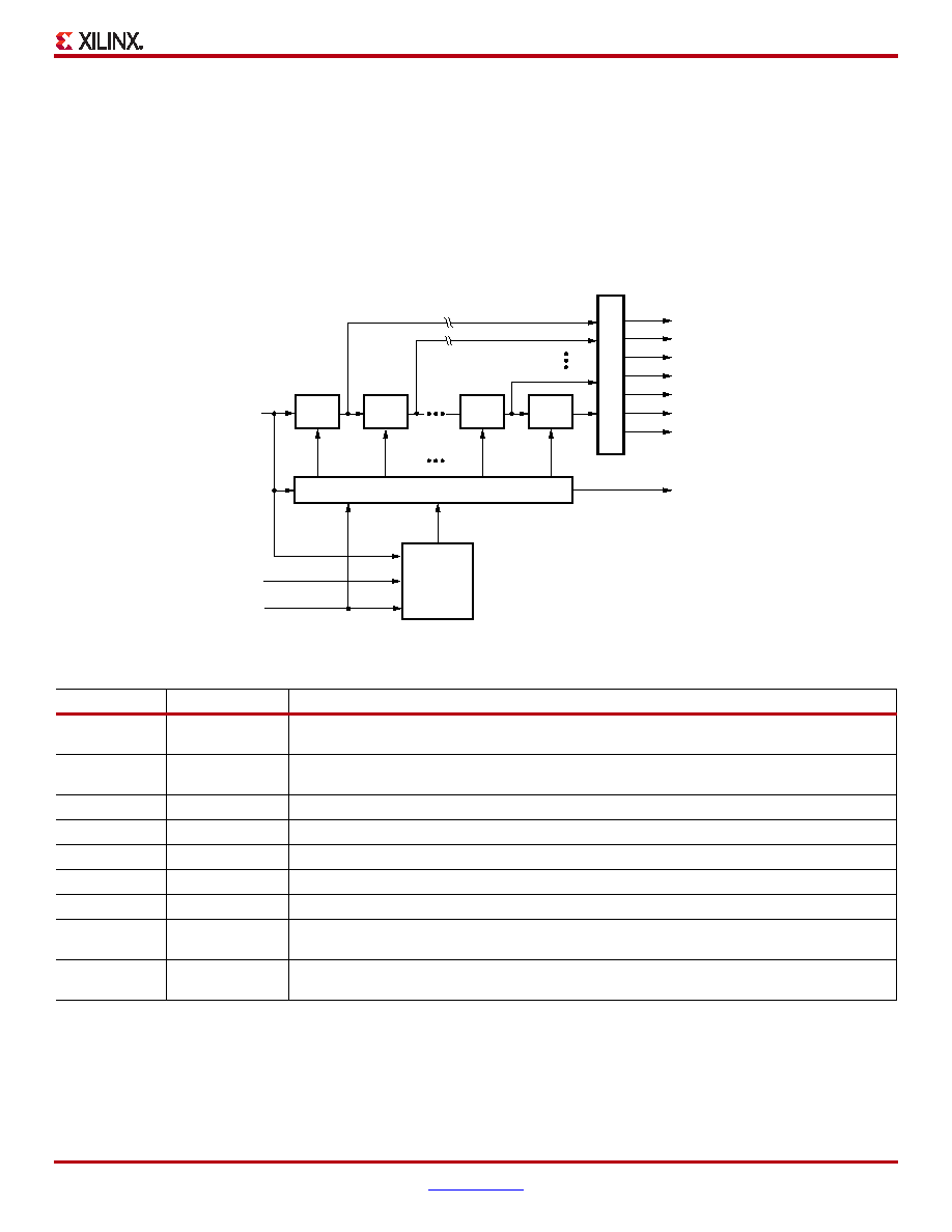
Delay-Locked Loop (DLL)
The most basic function of the DLL component is to
eliminate clock skew. The main signal path of the DLL
consists of an input stage, followed by a series of discrete
delay elements or steps, which in turn leads to an output
stage. This path together with logic for phase detection and
control forms a system complete with feedback as shown in
Figure 41. In Spartan-3E FPGAs, the DLL is implemented
using a counter-based delay line.
The DLL component has two clock inputs, CLKIN and
CLKFB, as well as seven clock outputs, CLK0, CLK90,
CLK180, CLK270, CLK2X, CLK2X180, and CLKDV as
described in Table 28. The clock outputs drive
simultaneously. Signals that initialize and report the state of
the DLL are discussed in Status Logic.
The clock signal supplied to the CLKIN input serves as a
reference waveform. The DLL seeks to align the rising-edge
of feedback signal at the CLKFB input with the rising-edge
of CLKIN input. When eliminating clock skew, the common
approach to using the DLL is as follows: The CLK0 signal is
passed through the clock distribution network that feeds all
the registers it synchronizes. These registers are either
internal or external to the FPGA. After passing through the
clock distribution network, the clock signal returns to the
DLL via a feedback line called CLKFB. The control block
inside the DLL measures the phase error between CLKFB
and CLKIN. This phase error is a measure of the clock skew
that the clock distribution network introduces. The control
block activates the appropriate number of delay steps to
X-Ref Target - Figure 41
Figure 41: Simplified Functional Diagram of DLL
Table 28: DLL Signals
Signal
Direction
Description
CLKIN
Input
inputs to a DCM.
CLKFB
Input
Accepts either CLK0 or CLK2X as the feedback signal. (Set the CLK_FEEDBACK attribute
accordingly).
CLK0
Output
Generates a clock signal with the same frequency and phase as CLKIN.
CLK90
Output
Generates a clock signal with the same frequency as CLKIN, phase-shifted by 90°.
CLK180
Output
Generates a clock signal with the same frequency as CLKIN, phase-shifted by 180°.
CLK270
Output
Generates a clock signal with the same frequency as CLKIN, phase-shifted by 270°.
CLK2X
Output
Generates a clock signal with the same phase as CLKIN, and twice the frequency.
CLK2X180
Output
Generates a clock signal with twice the frequency of CLKIN, and phase-shifted 180° with respect
to CLK2X.
CLKDV
Output
Divides the CLKIN frequency by CLKDV_DIVIDE value to generate lower frequency clock signal
that is phase-aligned to CLKIN.
DS099-2_08_041103
CLKIN
Delay
n
CLKFB
RST
CLK0
CLK90
CLK180
CLK270
CLK2X
CLK2X180
CLKDV
O
u
tp
u
tSection
Control
Delay
n-1
Phase
Detection
LOCKED
Delay
2
Delay
1
相关PDF资料 |
PDF描述 |
|---|---|
| AMM18DRMI | CONN EDGECARD 36POS .156 WW |
| TACR476K003R | CAP TANT 47UF 3V 10% 0805 |
| XC3S250E-4TQG144C | IC SPARTAN-3E FPGA 250K 144TQFP |
| RSA40DRMI-S288 | CONN EDGECARD 80POS .125 EXTEND |
| XC2S50-5FGG256C | IC SPARTAN-II FPGA 50K 256-FBGA |
相关代理商/技术参数 |
参数描述 |
|---|---|
| XC3S250E-4CPG132C4022 | 制造商:Xilinx 功能描述: |
| XC3S250E-4CPG132I | 功能描述:IC FPGA SPARTAN-3E 250K 132CSBGA RoHS:是 类别:集成电路 (IC) >> 嵌入式 - FPGA(现场可编程门阵列) 系列:Spartan®-3E 标准包装:40 系列:Spartan® 6 LX LAB/CLB数:3411 逻辑元件/单元数:43661 RAM 位总计:2138112 输入/输出数:358 门数:- 电源电压:1.14 V ~ 1.26 V 安装类型:表面贴装 工作温度:-40°C ~ 100°C 封装/外壳:676-BGA 供应商设备封装:676-FBGA(27x27) |
| XC3S250E-4FG320C | 制造商:XILINX 制造商全称:XILINX 功能描述:Spartan-3E FPGA Family |
| XC3S250E-4FG320I | 制造商:XILINX 制造商全称:XILINX 功能描述:Spartan-3E FPGA Family |
| XC3S250E-4FG400C | 制造商:XILINX 制造商全称:XILINX 功能描述:Spartan-3E FPGA Family |
发布紧急采购,3分钟左右您将得到回复。