参数资料
| 型号: | XC3S250E-5CPG132C |
| 厂商: | Xilinx Inc |
| 文件页数: | 172/227页 |
| 文件大小: | 0K |
| 描述: | IC FPGA SPARTAN-3E 250K 132CSBGA |
| 标准包装: | 360 |
| 系列: | Spartan®-3E |
| LAB/CLB数: | 612 |
| 逻辑元件/单元数: | 5508 |
| RAM 位总计: | 221184 |
| 输入/输出数: | 92 |
| 门数: | 250000 |
| 电源电压: | 1.14 V ~ 1.26 V |
| 安装类型: | 表面贴装 |
| 工作温度: | 0°C ~ 85°C |
| 封装/外壳: | 132-TFBGA,CSPBGA |
| 供应商设备封装: | 132-CSPBGA(8x8) |
第1页第2页第3页第4页第5页第6页第7页第8页第9页第10页第11页第12页第13页第14页第15页第16页第17页第18页第19页第20页第21页第22页第23页第24页第25页第26页第27页第28页第29页第30页第31页第32页第33页第34页第35页第36页第37页第38页第39页第40页第41页第42页第43页第44页第45页第46页第47页第48页第49页第50页第51页第52页第53页第54页第55页第56页第57页第58页第59页第60页第61页第62页第63页第64页第65页第66页第67页第68页第69页第70页第71页第72页第73页第74页第75页第76页第77页第78页第79页第80页第81页第82页第83页第84页第85页第86页第87页第88页第89页第90页第91页第92页第93页第94页第95页第96页第97页第98页第99页第100页第101页第102页第103页第104页第105页第106页第107页第108页第109页第110页第111页第112页第113页第114页第115页第116页第117页第118页第119页第120页第121页第122页第123页第124页第125页第126页第127页第128页第129页第130页第131页第132页第133页第134页第135页第136页第137页第138页第139页第140页第141页第142页第143页第144页第145页第146页第147页第148页第149页第150页第151页第152页第153页第154页第155页第156页第157页第158页第159页第160页第161页第162页第163页第164页第165页第166页第167页第168页第169页第170页第171页当前第172页第173页第174页第175页第176页第177页第178页第179页第180页第181页第182页第183页第184页第185页第186页第187页第188页第189页第190页第191页第192页第193页第194页第195页第196页第197页第198页第199页第200页第201页第202页第203页第204页第205页第206页第207页第208页第209页第210页第211页第212页第213页第214页第215页第216页第217页第218页第219页第220页第221页第222页第223页第224页第225页第226页第227页
Spartan-3E FPGA Family: Functional Description
DS312 (v4.1) July 19, 2013
Product Specification
49
cancel out the clock skew. When the DLL phase-aligns the
CLK0 signal with the CLKIN signal, it asserts the LOCKED
output, indicating a lock on to the CLKIN signal.
DLL Attributes and Related Functions
The DLL unit has a variety of associated attributes as
described in Table 29. Each attribute is described in detail in
the sections that follow.
DLL Clock Input Connections
For best results, an external clock source enters the FPGA
via a Global Clock Input (GCLK). Each specific DCM has
four possible direct, optimal GCLK inputs that feed the
DCM’s CLKIN input, as shown in Table 30. Table 30 also
provides the specific pin numbers by package for each
GCLK input. The two additional DCM’s on the XC3S1200E
and XC3S1600E have similar optimal connections from the
left-edge LHCLK and the right-edge RHCLK inputs, as
The DCM supports differential clock inputs (for
example, LVDS, LVPECL_25) via a pair of GCLK inputs
that feed an internal single-ended signal to the DCM’s
CLKIN input.
Design Note
Avoid using global clock input GCLK1 as it is always shared
with the M2 mode select pin. Global clock inputs GCLK0,
GCLK2, GCLK3, GCLK12, GCLK13, GCLK14, and
GCLK15 have shared functionality in some configuration
modes.
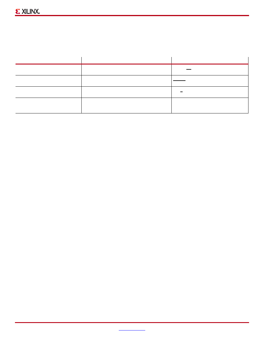
Table 29: DLL Attributes
Attribute
Description
Values
CLK_FEEDBACK
Chooses either the CLK0 or CLK2X output to drive
the CLKFB input
NONE, 1X, 2X
CLKIN_DIVIDE_BY_2
Halves the frequency of the CLKIN signal just as it
enters the DCM
FALSE, TRUE
CLKDV_DIVIDE
Selects the constant used to divide the CLKIN input
frequency to generate the CLKDV output frequency
1.5, 2, 2.5, 3, 3.5, 4, 4.5, 5, 5.5, 6.0, 6.5, 7.0,
7.5, 8, 9, 10, 11, 12, 13, 14, 15, and 16
CLKIN_PERIOD
Additional information that allows the DLL to
operate with the most efficient lock time and the
best jitter tolerance
Floating-point value representing the
CLKIN period in nanoseconds
相关PDF资料 |
PDF描述 |
|---|---|
| 34VL02T/MS | IC EEPROM 2KBIT 400KHZ 8MSOP |
| XC3S250E-4TQG144I | IC FPGA SPARTAN-3E 250K 144-TQFP |
| 34VL02T/MNY | IC EEPROM 2KBIT 400KHZ 8TDFN |
| XC3S250E-4CPG132I | IC FPGA SPARTAN-3E 250K 132CSBGA |
| XC2S50-6FG256C | IC FPGA 2.5V C-TEMP 256-FBGA |
相关代理商/技术参数 |
参数描述 |
|---|---|
| XC3S250E-5CPG132C4124 | 制造商:Xilinx 功能描述: |
| XC3S250E-5CPG132I | 制造商:XILINX 制造商全称:XILINX 功能描述:Spartan-3E FPGA Family |
| XC3S250E-5FG320C | 制造商:XILINX 制造商全称:XILINX 功能描述:Spartan-3E FPGA Family |
| XC3S250E-5FG320I | 制造商:XILINX 制造商全称:XILINX 功能描述:Spartan-3E FPGA Family |
| XC3S250E-5FG400C | 制造商:XILINX 制造商全称:XILINX 功能描述:Spartan-3E FPGA Family |
发布紧急采购,3分钟左右您将得到回复。