参数资料
| 型号: | XC4005E-1PQ160C |
| 厂商: | Xilinx Inc |
| 文件页数: | 32/68页 |
| 文件大小: | 0K |
| 描述: | IC FPGA C-TEMP 5V 1-SPD 160-PQFP |
| 产品变化通告: | Product Discontinuation 28/Jul/2010 |
| 标准包装: | 24 |
| 系列: | XC4000E/X |
| LAB/CLB数: | 196 |
| 逻辑元件/单元数: | 466 |
| RAM 位总计: | 6272 |
| 输入/输出数: | 112 |
| 门数: | 5000 |
| 电源电压: | 4.75 V ~ 5.25 V |
| 安装类型: | 表面贴装 |
| 工作温度: | 0°C ~ 85°C |
| 封装/外壳: | 160-BQFP |
| 供应商设备封装: | 160-PQFP(28x28) |
第1页第2页第3页第4页第5页第6页第7页第8页第9页第10页第11页第12页第13页第14页第15页第16页第17页第18页第19页第20页第21页第22页第23页第24页第25页第26页第27页第28页第29页第30页第31页当前第32页第33页第34页第35页第36页第37页第38页第39页第40页第41页第42页第43页第44页第45页第46页第47页第48页第49页第50页第51页第52页第53页第54页第55页第56页第57页第58页第59页第60页第61页第62页第63页第64页第65页第66页第67页第68页
R
XC4000E and XC4000X Series Field Programmable Gate Arrays
6-42
May 14, 1999 (Version 1.6)
Boundary Scan
The ‘bed of nails’ has been the traditional method of testing
electronic assemblies. This approach has become less
appropriate, due to closer pin spacing and more sophisti-
cated assembly methods like surface-mount technology
and multi-layer boards. The IEEE Boundary Scan Standard
1149.1 was developed to facilitate board-level testing of
electronic assemblies. Design and test engineers can
imbed a standard test logic structure in their device to
achieve high fault coverage for I/O and internal logic. This
structure is easily implemented with a four-pin interface on
any boundary scan-compatible IC. IEEE 1149.1-compati-
ble devices may be serial daisy-chained together, con-
nected in parallel, or a combination of the two.
The XC4000 Series implements IEEE 1149.1-compatible
BYPASS, PRELOAD/SAMPLE and EXTEST boundary
scan instructions. When the boundary scan conguration
option is selected, three normal user I/O pins become ded-
icated inputs for these functions. Another user output pin
becomes the dedicated boundary scan output. The details
of how to enable this circuitry are covered later in this sec-
tion.
By exercising these input signals, the user can serially load
commands and data into these devices to control the driv-
ing of their outputs and to examine their inputs. This
method is an improvement over bed-of-nails testing. It
avoids the need to over-drive device outputs, and it reduces
the user interface to four pins. An optional fth pin, a reset
for the control logic, is described in the standard but is not
implemented in Xilinx devices.
The dedicated on-chip logic implementing the IEEE 1149.1
functions includes a 16-state machine, an instruction regis-
ter and a number of data registers. The functional details
can be found in the IEEE 1149.1 specication and are also
discussed in the Xilinx application note XAPP 017: “
Bound-
ary Scan in XC4000 Devices.”
Figure 40 on page 43 shows a simplied block diagram of
the XC4000E Input/Output Block with boundary scan
implemented. XC4000X boundary scan logic is identical.
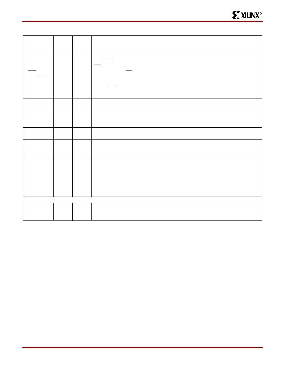
CS0, CS1,
WS, RS
I
I/O
These four inputs are used in Asynchronous Peripheral mode. The chip is selected
when CS0 is Low and CS1 is High. While the chip is selected, a Low on Write Strobe
(WS) loads the data present on the D0 - D7 inputs into the internal data buffer. A Low
on Read Strobe (RS) changes D7 into a status output — High if Ready, Low if Busy —
and drives D0 - D6 High.
In Express mode, CS1 is used as a serial-enable signal for daisy-chaining.
WS and RS should be mutually exclusive, but if both are Low simultaneously, the Write
Strobe overrides. After configuration, these are user-programmable I/O pins.
A0 - A17
O
I/O
During Master Parallel configuration, these 18 output pins address the configuration
EPROM. After configuration, they are user-programmable I/O pins.
A18 - A21
(XC4003XL to
XC4085XL)
O
I/O
During Master Parallel configuration with an XC4000X master, these 4 output pins add
4 more bits to address the configuration EPROM. After configuration, they are user-pro-
grammable I/O pins. (See Master Parallel Configuration section for additional details.)
D0 - D7
I
I/O
During Master Parallel and Peripheral configuration, these eight input pins receive con-
figuration data. After configuration, they are user-programmable I/O pins.
DIN
I
I/O
During Slave Serial or Master Serial configuration, DIN is the serial configuration data
input receiving data on the rising edge of CCLK. During Parallel configuration, DIN is
the D0 input. After configuration, DIN is a user-programmable I/O pin.
DOUT
O
I/O
During configuration in any mode but Express mode, DOUT is the serial configuration
data output that can drive the DIN of daisy-chained slave FPGAs. DOUT data changes
on the falling edge of CCLK, one-and-a-half CCLK periods after it was received at the
DIN input.
In Express modefor XC4000E and XC4000X only, DOUT is the status output that can
drive the CS1 of daisy-chained FPGAs, to enable and disable downstream devices.
After configuration, DOUT is a user-programmable I/O pin.
Unrestricted User-Programmable I/O Pins
I/O
Weak
Pull-up
I/O
These pins can be configured to be input and/or output after configuration is completed.
Before configuration is completed, these pins have an internal high-value pull-up resis-
tor (25 k
- 100 k) that defines the logic level as High.
Table 16: Pin Descriptions (Continued)
Pin Name
I/O
During
Cong.
I/O
After
Cong.
Pin Description
Product Obsolete or Under Obsolescence
相关PDF资料 |
PDF描述 |
|---|---|
| XC4003E-3VQ100I | IC FPGA I-TEMP 5V 3SPD 100-VQFP |
| XC4003E-3VQ100C | IC FPGA C-TEMP 5V 3SPD 100-VQFP |
| XC4010E-3PQ160C | IC FPGA 400 CLB'S 160-PQFP |
| AMC43DREH-S734 | CONN EDGECARD 86POS .100 EYELET |
| RSC35DTEF | CONN EDGECARD 70POS .100 EYELET |
相关代理商/技术参数 |
参数描述 |
|---|---|
| XC4005E-1PQ160I | 制造商:未知厂家 制造商全称:未知厂家 功能描述:Field Programmable Gate Array (FPGA) |
| XC4005E-1PQ208C | 功能描述:IC FPGA C-TEMP 5V 1-SPD 208-PQFP RoHS:否 类别:集成电路 (IC) >> 嵌入式 - FPGA(现场可编程门阵列) 系列:XC4000E/X 标准包装:1 系列:Kintex-7 LAB/CLB数:25475 逻辑元件/单元数:326080 RAM 位总计:16404480 输入/输出数:350 门数:- 电源电压:0.97 V ~ 1.03 V 安装类型:表面贴装 工作温度:0°C ~ 85°C 封装/外壳:900-BBGA,FCBGA 供应商设备封装:900-FCBGA(31x31) 其它名称:122-1789 |
| XC4005E-1PQ208I | 制造商:未知厂家 制造商全称:未知厂家 功能描述:Field Programmable Gate Array (FPGA) |
| XC4005E-1TQ144C | 功能描述:IC FPGA C-TEMP 5V 1-SPD 144-TQFP RoHS:否 类别:集成电路 (IC) >> 嵌入式 - FPGA(现场可编程门阵列) 系列:XC4000E/X 标准包装:1 系列:Kintex-7 LAB/CLB数:25475 逻辑元件/单元数:326080 RAM 位总计:16404480 输入/输出数:350 门数:- 电源电压:0.97 V ~ 1.03 V 安装类型:表面贴装 工作温度:0°C ~ 85°C 封装/外壳:900-BBGA,FCBGA 供应商设备封装:900-FCBGA(31x31) 其它名称:122-1789 |
| XC4005E-1TQ144I | 制造商:未知厂家 制造商全称:未知厂家 功能描述:Field Programmable Gate Array (FPGA) |
发布紧急采购,3分钟左右您将得到回复。