- 您现在的位置:买卖IC网 > PDF目录221636 > XC4005E-1PQG100C (XILINX INC) FPGA, 196 CLBS, 3000 GATES, 166 MHz, PQFP100 PDF资料下载
参数资料
| 型号: | XC4005E-1PQG100C |
| 厂商: | XILINX INC |
| 元件分类: | FPGA |
| 英文描述: | FPGA, 196 CLBS, 3000 GATES, 166 MHz, PQFP100 |
| 文件页数: | 11/17页 |
| 文件大小: | 75K |
| 代理商: | XC4005E-1PQG100C |
R
February 11, 2000 (Version 1.8)
6-103
XC4000E and XC4000X Series Field Programmable Gate Arrays
6
XC4000E Switching Characteristics
Testing of the switching parameters is modeled after testing methods specied by MIL-M-38510/605. All devices are 100%
functionally tested. Internal timing parameters are derived from measuring internal test patterns. Listed below are
representative values where one global clock input drives one vertical clock line in each accessible column, and where all
accessible IOB and CLB ip-ops are clocked by the global clock net.
When fewer vertical clock lines are connected, the clock distribution is faster; when multiple clock lines per column are driven
from the same global clock, the delay is longer. For more specic, more precise, and worst-case guaranteed data, reecting
the actual routing structure, use the values provided by the static timing analyzer (TRCE in the Xilinx Development System)
and back-annotated to the simulation net list. These path delays, provided as a guideline, have been extracted from the
static timing analyzer report. All timing parameters assume worst-case operating conditions (supply voltage and junction
temperature).
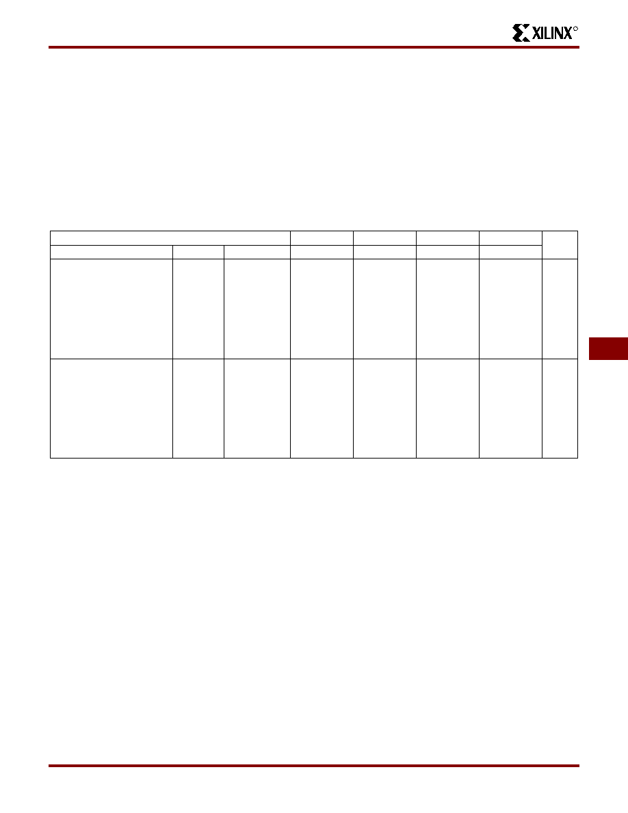
Global Buffer Switching Characteristic Guidelines
Speed Grade
-4
-3
-2
-1
Units
Description
Symbol
Device
Max
From pad through
Primary buffer,
to any clock K
TPG
XC4003E
XC4005E
XC4006E
XC4008E
XC4010E
XC4013E
XC4020E
XC4025E
7.0
7.5
8.0
11.0
11.5
12.0
12.5
4.7
5.3
6.1
6.3
6.8
7.0
7.2
4.0
4.3
5.2
5.4
5.8
6.4
6.9
3.5
3.8
4.6
4.8
5.2
6.0
–
ns
From pad through
Secondary buffer,
to any clock K
TSG
XC4003E
XC4005E
XC4006E
XC4008E
XC4010E
XC4013E
XC4020E
XC4025E
7.5
8.0
8.5
11.5
12.0
12.5
13.0
5.2
5.8
6.6
6.8
7.3
7.5
7.7
4.4
4.7
5.6
5.8
6.2
6.7
7.2
4.0
4.3
5.1
5.3
5.7
6.5
–
ns
相关PDF资料 |
PDF描述 |
|---|---|
| XC4005E-2PQG100C | FPGA, 196 CLBS, 3000 GATES, 125 MHz, PQFP100 |
| XC4005E-2PQG100I | FPGA, 196 CLBS, 3000 GATES, 125 MHz, PQFP100 |
| XC4005E-3PQG100C | FPGA, 196 CLBS, 3000 GATES, 125 MHz, PQFP100 |
| XC4005E-3PQG100I | FPGA, 196 CLBS, 3000 GATES, 125 MHz, PQFP100 |
| XC4005E-4PQG100C | FPGA, 196 CLBS, 3000 GATES, 111 MHz, PQFP100 |
相关代理商/技术参数 |
参数描述 |
|---|---|
| XC4005E-1TQ144C | 功能描述:IC FPGA C-TEMP 5V 1-SPD 144-TQFP RoHS:否 类别:集成电路 (IC) >> 嵌入式 - FPGA(现场可编程门阵列) 系列:XC4000E/X 标准包装:1 系列:Kintex-7 LAB/CLB数:25475 逻辑元件/单元数:326080 RAM 位总计:16404480 输入/输出数:350 门数:- 电源电压:0.97 V ~ 1.03 V 安装类型:表面贴装 工作温度:0°C ~ 85°C 封装/外壳:900-BBGA,FCBGA 供应商设备封装:900-FCBGA(31x31) 其它名称:122-1789 |
| XC4005E-1TQ144I | 制造商:未知厂家 制造商全称:未知厂家 功能描述:Field Programmable Gate Array (FPGA) |
| XC4005E-2PC84C | 功能描述:IC FPGA C-TEMP 5V 2-SPD 84-PLCC RoHS:否 类别:集成电路 (IC) >> 嵌入式 - FPGA(现场可编程门阵列) 系列:XC4000E/X 标准包装:1 系列:Kintex-7 LAB/CLB数:25475 逻辑元件/单元数:326080 RAM 位总计:16404480 输入/输出数:350 门数:- 电源电压:0.97 V ~ 1.03 V 安装类型:表面贴装 工作温度:0°C ~ 85°C 封装/外壳:900-BBGA,FCBGA 供应商设备封装:900-FCBGA(31x31) 其它名称:122-1789 |
| XC4005E-2PC84I | 功能描述:IC FPGA I-TEMP 5V 2-SPD 84-PLCC RoHS:否 类别:集成电路 (IC) >> 嵌入式 - FPGA(现场可编程门阵列) 系列:XC4000E/X 标准包装:1 系列:Kintex-7 LAB/CLB数:25475 逻辑元件/单元数:326080 RAM 位总计:16404480 输入/输出数:350 门数:- 电源电压:0.97 V ~ 1.03 V 安装类型:表面贴装 工作温度:0°C ~ 85°C 封装/外壳:900-BBGA,FCBGA 供应商设备封装:900-FCBGA(31x31) 其它名称:122-1789 |
| XC4005E-2PG156C | 功能描述:IC FPGA C-TEMP 5V 2-SPD 156-CPGA RoHS:否 类别:集成电路 (IC) >> 嵌入式 - FPGA(现场可编程门阵列) 系列:XC4000E/X 标准包装:1 系列:Kintex-7 LAB/CLB数:25475 逻辑元件/单元数:326080 RAM 位总计:16404480 输入/输出数:350 门数:- 电源电压:0.97 V ~ 1.03 V 安装类型:表面贴装 工作温度:0°C ~ 85°C 封装/外壳:900-BBGA,FCBGA 供应商设备封装:900-FCBGA(31x31) 其它名称:122-1789 |
发布紧急采购,3分钟左右您将得到回复。