- 您现在的位置:买卖IC网 > PDF目录221637 > XC4005E-4PQG208I (XILINX INC) FPGA, 196 CLBS, 3000 GATES, 111 MHz, PQFP208 PDF资料下载
参数资料
| 型号: | XC4005E-4PQG208I |
| 厂商: | XILINX INC |
| 元件分类: | FPGA |
| 英文描述: | FPGA, 196 CLBS, 3000 GATES, 111 MHz, PQFP208 |
| 文件页数: | 7/17页 |
| 文件大小: | 75K |
| 代理商: | XC4005E-4PQG208I |
R
February 11, 2000 (Version 1.8)
6-115
XC4000E and XC4000X Series Field Programmable Gate Arrays
6
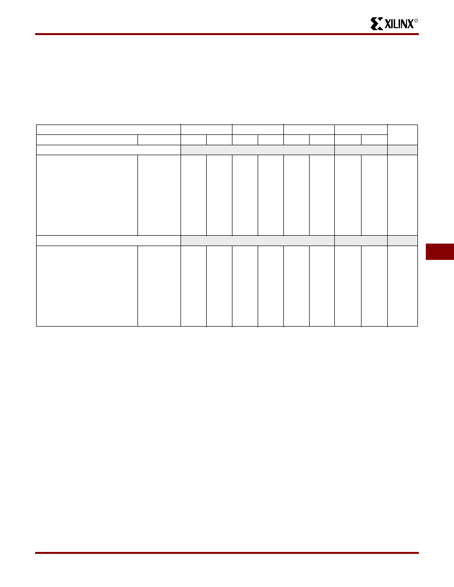
XC4000E IOB Output Switching Characteristic Guidelines
Testing of switching parameters is modeled after testing methods specied by MIL-M-38510/605. All devices are 100%
functionally tested. Internal timing parameters are derived from measuring internal test patterns. Listed below are
representative values. For more specic, more precise, and worst-case guaranteed data, use the values reported by the
static timing analyzer (TRCE in the Xilinx Development System) and back-annotated to the simulation net list. These path
delays, provided as a guideline, have been extracted from the static timing analyzer report. All timing parameters assume
worst-case operating conditions (supply voltage and junction temperature). Values apply to all XC4000E devices unless
otherwise noted.
Speed Grade
-4
-3
-2
-1
Units
Description
Symbol
Min
Max
Min
Max
Min
Max
Min
Max
Propagation Delays (TTL Output Levels)
Clock (OK) to Pad, fast
slew-rate limited
Output (O) to Pad, fast
slew-rate limited
3-state to Pad hi-Z
(slew-rate independent)
3-state to Pad active
and valid, fast
slew-rate limited
TOKPOF
TOKPOS
TOPF
TOPS
TTSHZ
TTSONF
TTSONS
7.5
11.5
8.0
12.0
5.0
9.7
13.7
6.5
9.5
5.5
8.5
4.2
8.1
11.1
4.5
7.0
4.8
7.3
3.8
7.3
9.8
3.0
5.0
3.2
5.2
3.0
6.8
8.8
ns
Propagation Delays (CMOS Output Levels)
Clock (OK) to Pad, fast
slew-rate limited
Output (O) to Pad, fast
slew-rate limited
3-state to Pad hi-Z
(slew-rate independent)
3-state to Pad active
and valid, fast
slew-rate limited
TOKPOFC
TOKPOSC
TOPFC
TOPSC
TTSHZC
TTSONFC
TTSONSC
9.5
13.5
10.0
14.0
5.2
9.1
13.1
7.8
11.6
9.7
13.4
4.3
7.6
11.4
7.0
10.4
8.7
12.1
3.9
6.8
10.2
4.0
7.0
4.0
6.0
3.9
6.8
8.8
ns
Note 1:
Output timing is measured at pin threshold, with 50pF external capacitive loads (incl. test xture). Slew-rate limited output
rise/fall times are approximately two times longer than fast output rise/fall times. For the effect of capacitive loads on ground
bounce, see the “Additional XC4000 Data” section of the Programmable Logic Data Book.
Note 2:
Voltage levels of unused pads, bonded or unbonded, must be valid logic levels. Each can be congured with the internal
pull-up (default) or pull-down resistor, or congured as a driven output, or can be driven from an external source.
相关PDF资料 |
PDF描述 |
|---|---|
| X25645V14I-2.7 | 1-CHANNEL POWER SUPPLY MANAGEMENT CKT, PDSO14 |
| X25645S8I | 1-CHANNEL POWER SUPPLY MANAGEMENT CKT, PDSO8 |
| XWD2415-TS93V | 2-OUTPUT 150 W DC-DC REG PWR SUPPLY MODULE |
| XWD4805-TS1V | 2-OUTPUT 150 W DC-DC REG PWR SUPPLY MODULE |
| X25325V14I | 1-CHANNEL POWER SUPPLY MANAGEMENT CKT, PDSO14 |
相关代理商/技术参数 |
参数描述 |
|---|---|
| XC4005E-4TQ144C | 功能描述:IC FPGA C-TEMP 5V 4-SPD 144-TQFP RoHS:否 类别:集成电路 (IC) >> 嵌入式 - FPGA(现场可编程门阵列) 系列:XC4000E/X 标准包装:1 系列:Kintex-7 LAB/CLB数:25475 逻辑元件/单元数:326080 RAM 位总计:16404480 输入/输出数:350 门数:- 电源电压:0.97 V ~ 1.03 V 安装类型:表面贴装 工作温度:0°C ~ 85°C 封装/外壳:900-BBGA,FCBGA 供应商设备封装:900-FCBGA(31x31) 其它名称:122-1789 |
| XC4005E-4TQ144I | 功能描述:IC FPGA I-TEMP 5V 4-SPD 144-TQFP RoHS:否 类别:集成电路 (IC) >> 嵌入式 - FPGA(现场可编程门阵列) 系列:XC4000E/X 标准包装:1 系列:Kintex-7 LAB/CLB数:25475 逻辑元件/单元数:326080 RAM 位总计:16404480 输入/输出数:350 门数:- 电源电压:0.97 V ~ 1.03 V 安装类型:表面贴装 工作温度:0°C ~ 85°C 封装/外壳:900-BBGA,FCBGA 供应商设备封装:900-FCBGA(31x31) 其它名称:122-1789 |
| XC4005H | 制造商:XILINX 制造商全称:XILINX 功能描述:Logic Cell Array Families |
| XC4005H-4MQ240C | 制造商:未知厂家 制造商全称:未知厂家 功能描述:Field Programmable Gate Array (FPGA) |
| XC4005H-4PG223C | 制造商:未知厂家 制造商全称:未知厂家 功能描述:Field Programmable Gate Array (FPGA) |
发布紧急采购,3分钟左右您将得到回复。