参数资料
| 型号: | XC4005XL-3PC84C |
| 厂商: | Xilinx Inc |
| 文件页数: | 53/68页 |
| 文件大小: | 0K |
| 描述: | IC FPGA C-TEMP 3.3V 3SPD 84-PLCC |
| 产品变化通告: | XC4000(XL,XLA,E) Discontinuation 15/Nov/2004 |
| 标准包装: | 15 |
| 系列: | XC4000E/X |
| LAB/CLB数: | 196 |
| 逻辑元件/单元数: | 466 |
| RAM 位总计: | 6272 |
| 输入/输出数: | 61 |
| 门数: | 5000 |
| 电源电压: | 3 V ~ 3.6 V |
| 安装类型: | 表面贴装 |
| 工作温度: | 0°C ~ 85°C |
| 封装/外壳: | 84-LCC(J 形引线) |
| 供应商设备封装: | 84-PLCC |
第1页第2页第3页第4页第5页第6页第7页第8页第9页第10页第11页第12页第13页第14页第15页第16页第17页第18页第19页第20页第21页第22页第23页第24页第25页第26页第27页第28页第29页第30页第31页第32页第33页第34页第35页第36页第37页第38页第39页第40页第41页第42页第43页第44页第45页第46页第47页第48页第49页第50页第51页第52页当前第53页第54页第55页第56页第57页第58页第59页第60页第61页第62页第63页第64页第65页第66页第67页第68页
R
May 14, 1999 (Version 1.6)
6-61
XC4000E and XC4000X Series Field Programmable Gate Arrays
6
Master Serial Mode
In Master Serial mode, the CCLK output of the lead FPGA
drives a Xilinx Serial PROM that feeds the FPGA DIN input.
Each rising edge of the CCLK output increments the Serial
PROM internal address counter. The next data bit is put on
the SPROM data output, connected to the FPGA DIN pin.
The lead FPGA accepts this data on the subsequent rising
CCLK edge.
The lead FPGA then presents the preamble data—and all
data that overows the lead device—on its DOUT pin.
There is an internal pipeline delay of 1.5 CCLK periods,
which means that DOUT changes on the falling CCLK
edge, and the next FPGA in the daisy chain accepts data
on the subsequent rising CCLK edge.
In the bitstream generation software, the user can specify
Fast CongRate, which, starting several bits into the rst
frame, increases the CCLK frequency by a factor of eight.
For actual timing values please refer to “Conguration
Switching Characteristics” on page 68. Be sure that the
serial PROM and slaves are fast enough to support this
data rate. XC2000, XC3000/A, and XC3100A devices do
not support the Fast CongRate option.
The SPROM CE input can be driven from either LDC or
DONE. Using LDC avoids potential contention on the DIN
pin, if this pin is congured as user-I/O, but LDC is then
restricted to be a permanently High user output after con-
guration. Using DONE can also avoid contention on DIN,
provided the early DONE option is invoked.
Figure 51 on page 60 shows a full master/slave system.
The leftmost device is in Master Serial mode.
Master Serial mode is selected by a <000> on the mode
pins (M2, M1, M0).
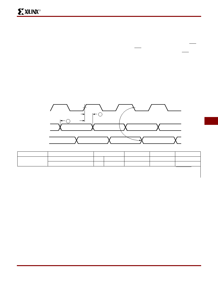
Figure 53: Master Serial Mode Programming Switching Characteristics
Description
Symbol
Min
Max
Units
CCLK
DIN setup
1
TDSCK
20
ns
DIN hold
2
TCKDS
0ns
Notes:
1. At power-up, Vcc must rise from 2.0 V to Vcc min in less than 25 ms, otherwise delay conguration by pulling PROGRAM
Low until Vcc is valid.
2. Master Serial mode timing is based on testing in slave mode.
Serial Data In
CCLK
(Output)
Serial DOUT
(Output)
1
TDSCK
2
TCKDS
n
n + 1
n + 2
n – 3
n – 2
n – 1
n
X3223
Product Obsolete or Under Obsolescence
相关PDF资料 |
PDF描述 |
|---|---|
| XC4005XL-2VQ100I | IC FPGA I-TEMP 3.3V 2SP 100VQFP |
| XC4005XL-2VQ100C | IC FPGA C-TEMP 3.3V 2SP 100VQFP |
| XC4005XL-2TQ144I | IC FPGA I-TEMP 3.3V 2SPD 144TQFP |
| ABB106DHRR-S621 | CONN EDGECARD EXTEND 212POS .050 |
| XC4005XL-2TQ144C | IC FPGA C-TEMP 3.3V 2SPD 144TQFP |
相关代理商/技术参数 |
参数描述 |
|---|---|
| XC4005XL-3PC84I | 功能描述:IC FPGA I-TEMP 3.3V 3SPD 84-PLCC RoHS:否 类别:集成电路 (IC) >> 嵌入式 - FPGA(现场可编程门阵列) 系列:XC4000E/X 标准包装:1 系列:Kintex-7 LAB/CLB数:25475 逻辑元件/单元数:326080 RAM 位总计:16404480 输入/输出数:350 门数:- 电源电压:0.97 V ~ 1.03 V 安装类型:表面贴装 工作温度:0°C ~ 85°C 封装/外壳:900-BBGA,FCBGA 供应商设备封装:900-FCBGA(31x31) 其它名称:122-1789 |
| XC4005XL-3PC84M | 制造商:XILINX 制造商全称:XILINX 功能描述:XC4000E and XC4000X Series Field Programmable Gate Arrays |
| XC4005XL-3PQ100C | 功能描述:IC FPGA C-TEMP 3.3V 3SPD 100PQFP RoHS:否 类别:集成电路 (IC) >> 嵌入式 - FPGA(现场可编程门阵列) 系列:XC4000E/X 标准包装:1 系列:Kintex-7 LAB/CLB数:25475 逻辑元件/单元数:326080 RAM 位总计:16404480 输入/输出数:350 门数:- 电源电压:0.97 V ~ 1.03 V 安装类型:表面贴装 工作温度:0°C ~ 85°C 封装/外壳:900-BBGA,FCBGA 供应商设备封装:900-FCBGA(31x31) 其它名称:122-1789 |
| XC4005XL-3PQ100I | 功能描述:IC FPGA I-TEMP 3.3V 3SPD 100PQFP RoHS:否 类别:集成电路 (IC) >> 嵌入式 - FPGA(现场可编程门阵列) 系列:XC4000E/X 标准包装:1 系列:Kintex-7 LAB/CLB数:25475 逻辑元件/单元数:326080 RAM 位总计:16404480 输入/输出数:350 门数:- 电源电压:0.97 V ~ 1.03 V 安装类型:表面贴装 工作温度:0°C ~ 85°C 封装/外壳:900-BBGA,FCBGA 供应商设备封装:900-FCBGA(31x31) 其它名称:122-1789 |
| XC4005XL-3PQ100M | 制造商:XILINX 制造商全称:XILINX 功能描述:XC4000E and XC4000X Series Field Programmable Gate Arrays |
发布紧急采购,3分钟左右您将得到回复。