参数资料
| 型号: | XC4006E-1PC84C |
| 厂商: | Xilinx Inc |
| 文件页数: | 13/68页 |
| 文件大小: | 0K |
| 描述: | IC FPGA C-TEMP 5V 1SPD 84-PLCC |
| 产品变化通告: | XC4000XL/E, XC9500XV, XC3100A Discontinuance 12/Apr/2010 |
| 标准包装: | 15 |
| 系列: | XC4000E/X |
| LAB/CLB数: | 256 |
| 逻辑元件/单元数: | 608 |
| RAM 位总计: | 8192 |
| 输入/输出数: | 61 |
| 门数: | 6000 |
| 电源电压: | 4.75 V ~ 5.25 V |
| 安装类型: | 表面贴装 |
| 工作温度: | 0°C ~ 85°C |
| 封装/外壳: | 84-LCC(J 形引线) |
| 供应商设备封装: | 84-PLCC |
第1页第2页第3页第4页第5页第6页第7页第8页第9页第10页第11页第12页当前第13页第14页第15页第16页第17页第18页第19页第20页第21页第22页第23页第24页第25页第26页第27页第28页第29页第30页第31页第32页第33页第34页第35页第36页第37页第38页第39页第40页第41页第42页第43页第44页第45页第46页第47页第48页第49页第50页第51页第52页第53页第54页第55页第56页第57页第58页第59页第60页第61页第62页第63页第64页第65页第66页第67页第68页
R
XC4000E and XC4000X Series Field Programmable Gate Arrays
6-24
May 14, 1999 (Version 1.6)
Any XC4000 Series 5-Volt device with its outputs cong-
ured in TTL mode can drive the inputs of any typical
3.3-Volt device. (For a detailed discussion of how to inter-
face between 5 V and 3.3 V devices, see the 3V Products
section of
The Programmable Logic Data Book.)
Supported destinations for XC4000 Series device outputs
are shown in Table 12.
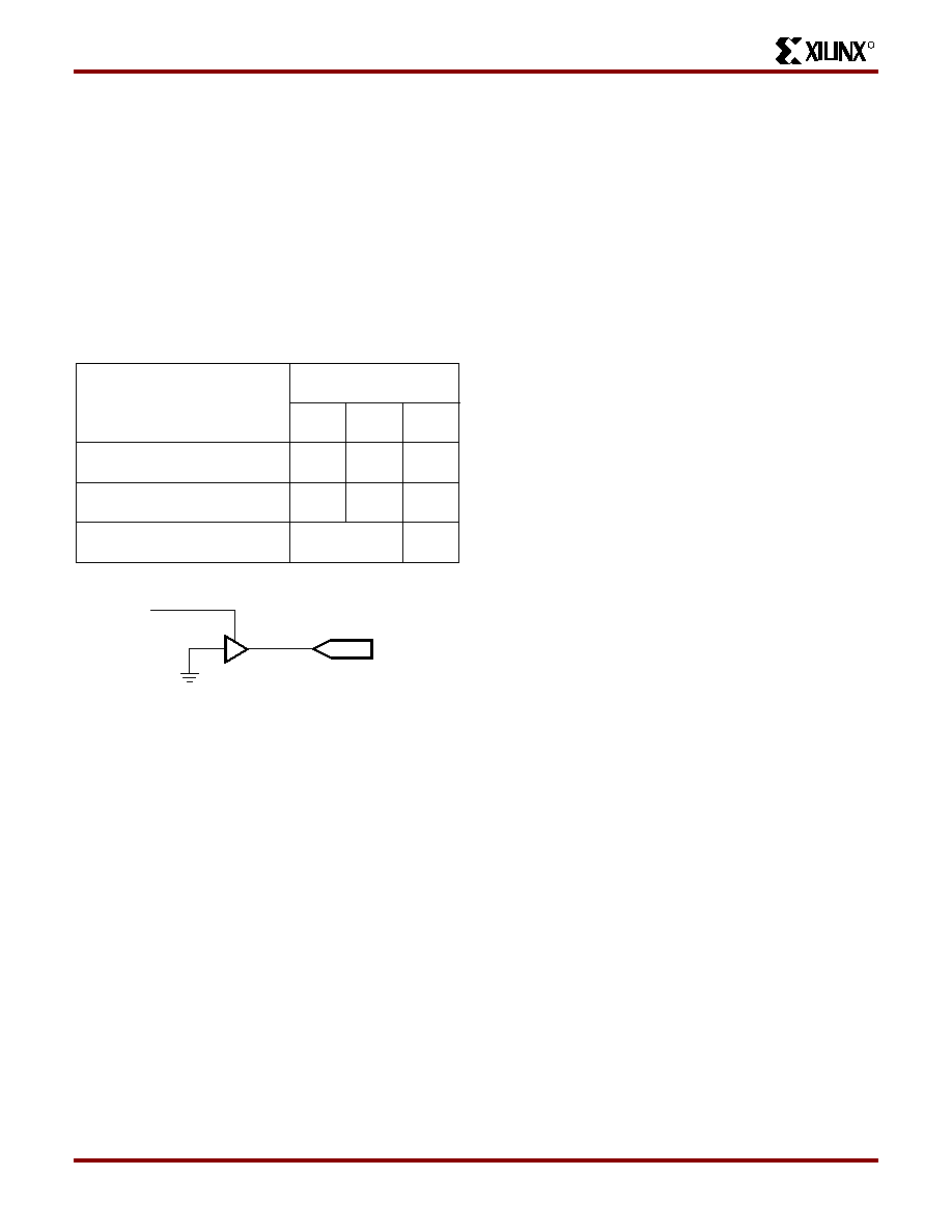
An output can be congured as open-drain (open-collector)
by placing an OBUFT symbol in a schematic or HDL code,
then tying the 3-state pin (T) to the output signal, and the
input pin (I) to Ground. (See Figure 18.)
Table 12: Supported Destinations for XC4000 Series
Outputs
Output Slew Rate
The slew rate of each output buffer is, by default, reduced,
to minimize power bus transients when switching non-criti-
cal signals. For critical signals, attach a FAST attribute or
property to the output buffer or ip-op.
For XC4000E devices, maximum total capacitive load for
simultaneous fast mode switching in the same direction is
200 pF for all package pins between each Power/Ground
pin
pair.
For
XC4000X
devices,
additional
internal
Power/Ground pin pairs are connected to special Power
and Ground planes within the packages, to reduce ground
bounce. Therefore, the maximum total capacitive load is
300 pF between each external Power/Ground pin pair.
Maximum loading may vary for the low-voltage devices.
For slew-rate limited outputs this total is two times larger for
each device type: 400 pF for XC4000E devices and 600 pF
for XC4000X devices. This maximum capacitive load
should not be exceeded, as it can result in ground bounce
of greater than 1.5 V amplitude and more than 5 ns dura-
tion. This level of ground bounce may cause undesired
transient behavior on an output, or in the internal logic. This
restriction is common to all high-speed digital ICs, and is
not particular to Xilinx or the XC4000 Series.
XC4000 Series devices have a feature called “Soft
Start-up,” designed to reduce ground bounce when all out-
puts are turned on simultaneously at the end of congura-
tion.
When the conguration process is nished and the
device starts up, the rst activation of the outputs is auto-
matically slew-rate limited. Immediately following the initial
activation of the I/O, the slew rate of the individual outputs
is determined by the individual conguration option for each
IOB.
Global Three-State
A separate Global 3-State line (not shown in Figure 15 or
Figure 16) forces all FPGA outputs to the high-impedance
state, unless boundary scan is enabled and is executing an
EXTEST instruction. This global net (GTS) does not com-
pete with other routing resources; it uses a dedicated distri-
bution network.
GTS can be driven from any user-programmable pin as a
global 3-state input. To use this global net, place an input
pad and input buffer in the schematic or HDL code, driving
the GTS pin of the STARTUP symbol. A specic pin loca-
tion can be assigned to this input using a LOC attribute or
property, just as with any other user-programmable pad. An
inverter can optionally be inserted after the input buffer to
invert the sense of the Global 3-State signal. Using GTS is
similar to GSR. See Figure 2 on page 11 for details.
Alternatively, GTS can be driven from any internal node.
Destination
XC4000 Series
Outputs
3.3 V,
CMOS
5 V,
TTL
5 V,
CMOS
Any typical device, Vcc = 3.3 V,
CMOS-threshold inputs
√√
some1
1. Only if destination device has 5-V tolerant inputs
Any device, Vcc = 5 V,
TTL-threshold inputs
√√√
Any device, Vcc = 5 V,
CMOS-threshold inputs
Unreliable
Data
√
X6702
OPAD
OBUFT
Figure 18: Open-Drain Output
Product Obsolete or Under Obsolescence
相关PDF资料 |
PDF描述 |
|---|---|
| XC4005XL-3VQ100I | IC FPGA I-TEMP 3.3V 3SP 100VQFP |
| ACC60DRYI-S13 | CONN EDGECARD 120POS .100 EXTEND |
| XC4006E-2PQ208C | IC FPGA C-TEMP 5V 2SPD 208-PQFP |
| XC4006E-2PQ160I | IC FPGA I-TEMP 5V 2SPD 160-PQFP |
| ASM43DSAN | CONN EDGECARD 86POS R/A .156 SLD |
相关代理商/技术参数 |
参数描述 |
|---|---|
| XC4006E-1PC84I | 制造商:未知厂家 制造商全称:未知厂家 功能描述:Field Programmable Gate Array (FPGA) |
| XC4006E-1PG156C | 功能描述:IC FPGA C-TEMP 5V 1SPD 156-CPGA RoHS:否 类别:集成电路 (IC) >> 嵌入式 - FPGA(现场可编程门阵列) 系列:XC4000E/X 标准包装:1 系列:Kintex-7 LAB/CLB数:25475 逻辑元件/单元数:326080 RAM 位总计:16404480 输入/输出数:350 门数:- 电源电压:0.97 V ~ 1.03 V 安装类型:表面贴装 工作温度:0°C ~ 85°C 封装/外壳:900-BBGA,FCBGA 供应商设备封装:900-FCBGA(31x31) 其它名称:122-1789 |
| XC4006E-1PG156I | 制造商:未知厂家 制造商全称:未知厂家 功能描述:Field Programmable Gate Array (FPGA) |
| XC4006E-1PG156M | 制造商:未知厂家 制造商全称:未知厂家 功能描述:Field Programmable Gate Array (FPGA) |
| XC4006E-1PQ160C | 功能描述:IC FPGA C-TEMP 5V 1SPD 160-PQFP RoHS:否 类别:集成电路 (IC) >> 嵌入式 - FPGA(现场可编程门阵列) 系列:XC4000E/X 标准包装:1 系列:Kintex-7 LAB/CLB数:25475 逻辑元件/单元数:326080 RAM 位总计:16404480 输入/输出数:350 门数:- 电源电压:0.97 V ~ 1.03 V 安装类型:表面贴装 工作温度:0°C ~ 85°C 封装/外壳:900-BBGA,FCBGA 供应商设备封装:900-FCBGA(31x31) 其它名称:122-1789 |
发布紧急采购,3分钟左右您将得到回复。