参数资料
| 型号: | XC4013E-2BG225C |
| 厂商: | Xilinx Inc |
| 文件页数: | 54/68页 |
| 文件大小: | 0K |
| 描述: | IC FPGA C-TEMP 5V 2SPD 225-PBGA |
| 产品变化通告: | Product Discontinuation 28/Jul/2010 |
| 标准包装: | 40 |
| 系列: | XC4000E/X |
| LAB/CLB数: | 576 |
| 逻辑元件/单元数: | 1368 |
| RAM 位总计: | 18432 |
| 输入/输出数: | 192 |
| 门数: | 13000 |
| 电源电压: | 4.75 V ~ 5.25 V |
| 安装类型: | 表面贴装 |
| 工作温度: | 0°C ~ 85°C |
| 封装/外壳: | 225-BBGA |
| 供应商设备封装: | 225-PBGA |
第1页第2页第3页第4页第5页第6页第7页第8页第9页第10页第11页第12页第13页第14页第15页第16页第17页第18页第19页第20页第21页第22页第23页第24页第25页第26页第27页第28页第29页第30页第31页第32页第33页第34页第35页第36页第37页第38页第39页第40页第41页第42页第43页第44页第45页第46页第47页第48页第49页第50页第51页第52页第53页当前第54页第55页第56页第57页第58页第59页第60页第61页第62页第63页第64页第65页第66页第67页第68页
R
XC4000E and XC4000X Series Field Programmable Gate Arrays
6-62
May 14, 1999 (Version 1.6)
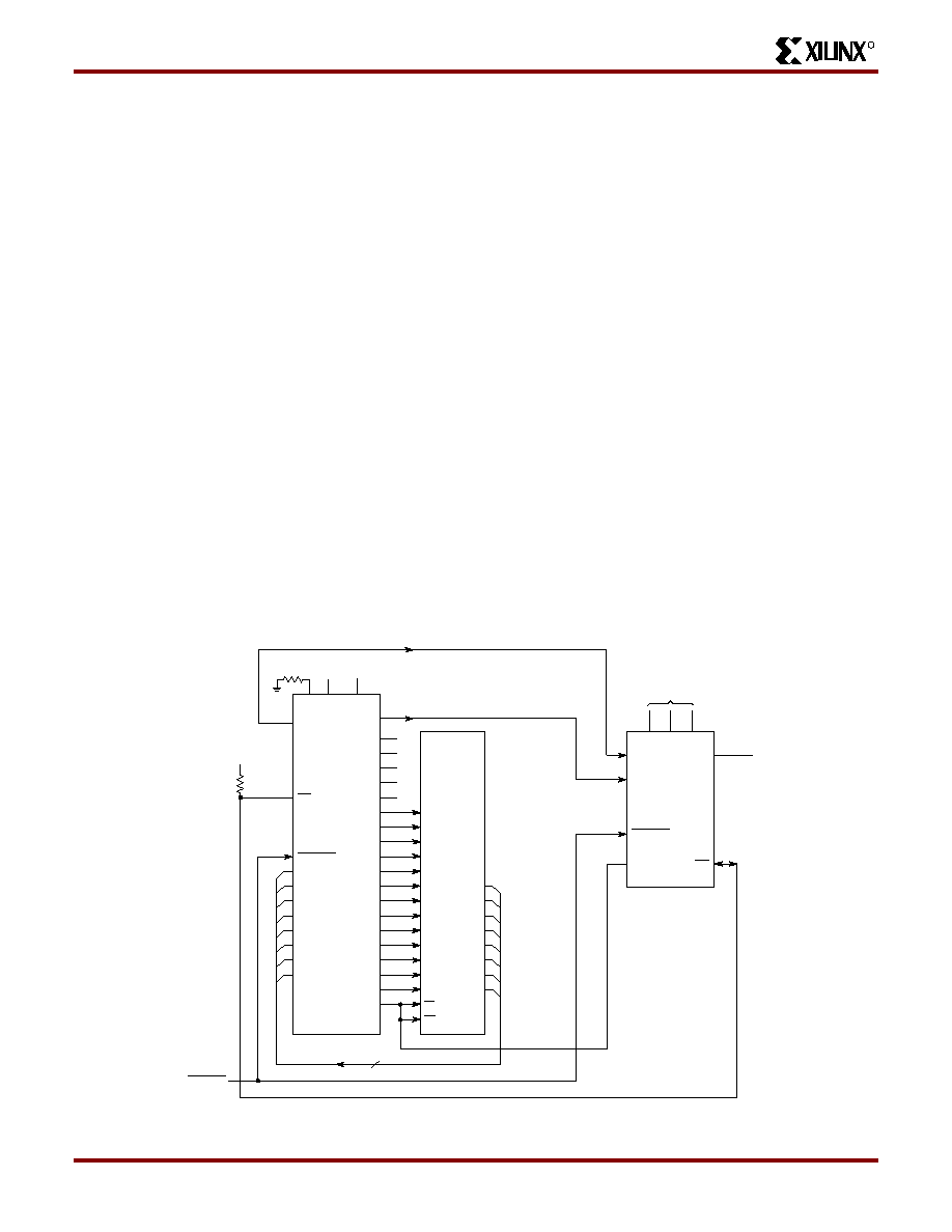
Master Parallel Modes
In the two Master Parallel modes, the lead FPGA directly
addresses an industry-standard byte-wide EPROM, and
accepts eight data bits just before incrementing or decre-
menting the address outputs.
The eight data bits are serialized in the lead FPGA, which
then presents the preamble data—and all data that over-
ows the lead device—on its DOUT pin. There is an inter-
nal delay of 1.5 CCLK periods, after the rising CCLK edge
that accepts a byte of data (and also changes the EPROM
address) until the falling CCLK edge that makes the LSB
(D0) of this byte appear at DOUT. This means that DOUT
changes on the falling CCLK edge, and the next FPGA in
the daisy chain accepts data on the subsequent rising
CCLK edge.
The PROM address pins can be incremented or decre-
mented, depending on the mode pin settings. This option
allows the FPGA to share the PROM with a wide variety of
microprocessors and micro controllers. Some processors
must boot from the bottom of memory (all zeros) while oth-
ers must boot from the top. The FPGA is exible and can
load its conguration bitstream from either end of the mem-
ory.
Master Parallel Up mode is selected by a <100> on the
mode pins (M2, M1, M0). The EPROM addresses start at
00000 and increment.
Master Parallel Down mode is selected by a <110> on the
mode pins. The EPROM addresses start at 3FFFF and
decrement.
Additional Address lines in XC4000 devices
The XC4000X devices have additional address lines
(A18-A21) allowing the additional address space required
to daisy-chain several large devices.
The extra address lines are programmable in XC4000EX
devices. By default these address lines are not activated. In
the default mode, the devices are compatible with existing
XC4000 and XC4000E products. If desired, the extra
address lines can be used by specifying the address lines
option in bitgen as 22 (bitgen -g AddressLines:22). The
lines (A18-A21) are driven when a master device detects,
via the bitstream, that it should be using all 22 address
lines. Because these pins will initially be pulled high by
internal pull-ups, designers using Master Parallel Up mode
should use external pull down resistors on pins A18-A21. If
Master Parallel Down mode is used external resistors are
not necessary.
All 22 address lines are always active in Master Parallel
modes with XC4000XL devices. The additional address
lines behave identically to the lower order address lines. If
the Address Lines option in bitgen is set to 18, it will be
ignored by the XC4000XL device.
The additional address lines (A18-A21) are not available in
the PC84 package.
M0
M1
DOUT
VCC
M2
PROGRAM
D7
D6
D5
D4
D3
D2
D1
D0
PROGRAM
CCLK
DIN
M0
M1
M2
DOUT
PROGRAM
EPROM
(8K x 8)
(OR LARGER)
A10
A11
A12
A9
A8
A7
A6
A5
A4
A3
A2
A1
A0
D7
DONE
D6
D5
D4
D3
D2
D1
D0
N/C
CE
OE
XC4000E/X
SLAVE
8
DATA BUS
CCLK
A15
A14
A13
A12
A11
A10
A9
A8
A7
A6
A5
A4
A3
A2
A1
A0
INIT
. . .
USER CONTROL OF HIGHER
ORDER PROM ADDRESS BITS
CAN BE USED TO SELECT BETWEEN
ALTERNATIVE CONFIGURATIONS
DONE
TO DIN OF OPTIONAL
DAISY-CHAINED FPGAS
A16
. . .
A17
. . .
HIGH
or
LOW
X9026
TO CCLK OF OPTIONAL
DAISY-CHAINED FPGAS
4.7K
4.7K
NOTE:M0 can be shorted
to Ground if not used
as I/O.
Figure 54: Master Parallel Mode Circuit Diagram
Product Obsolete or Under Obsolescence
相关PDF资料 |
PDF描述 |
|---|---|
| 485897-2 | CONN PLUG 4POS HOUSING W/DETENT |
| 1-487769-3 | 015 HOUSING FFC RCPT 100CL SR |
| IDT71V546XS100PFG | IC SRAM 4MBIT 100MHZ 100TQFP |
| 487769-4 | CONN RECEPT 6 POS .100 SLIMLINE |
| 15-38-8040 | CONN FFC FEMALE 4POS .100 TIN |
相关代理商/技术参数 |
参数描述 |
|---|---|
| XC4013E-2BG225I | 功能描述:IC FPGA I-TEMP 5V 2SPD 225-PBGA RoHS:否 类别:集成电路 (IC) >> 嵌入式 - FPGA(现场可编程门阵列) 系列:XC4000E/X 标准包装:1 系列:Kintex-7 LAB/CLB数:25475 逻辑元件/单元数:326080 RAM 位总计:16404480 输入/输出数:350 门数:- 电源电压:0.97 V ~ 1.03 V 安装类型:表面贴装 工作温度:0°C ~ 85°C 封装/外壳:900-BBGA,FCBGA 供应商设备封装:900-FCBGA(31x31) 其它名称:122-1789 |
| XC4013E-2BG240C | 制造商:XILINX 制造商全称:XILINX 功能描述:Programmable Gate Arrays |
| XC4013E-2BG240I | 制造商:XILINX 制造商全称:XILINX 功能描述:Programmable Gate Arrays |
| XC4013E-2BG240M | 制造商:XILINX 制造商全称:XILINX 功能描述:Programmable Gate Arrays |
| XC4013E-2CB240C | 制造商:XILINX 制造商全称:XILINX 功能描述:Programmable Gate Arrays |
发布紧急采购,3分钟左右您将得到回复。