- 您现在的位置:买卖IC网 > PDF目录300145 > XC4013E-3TQ240C (Xilinx, Inc.) XC4000E and XC4000X Series Field Programmable Gate Arrays PDF资料下载
参数资料
| 型号: | XC4013E-3TQ240C |
| 厂商: | Xilinx, Inc. |
| 英文描述: | XC4000E and XC4000X Series Field Programmable Gate Arrays |
| 中文描述: | XC4000E和XC4000X系列现场可编程门阵列 |
| 文件页数: | 3/4页 |
| 文件大小: | 21K |
| 代理商: | XC4013E-3TQ240C |
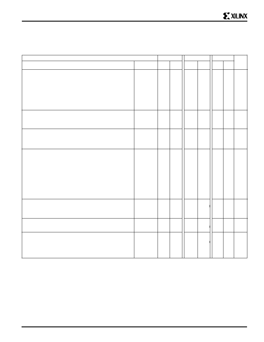
3
ADVANCE
INFORMATION
Speed Grade
-4
-3
-2
Description
Symbol
Min
Max
Min Max
Min Max Units
Input
Propagation Delays
Pad to I1, I2
TPID
2.5
ns
Pad to I1, I2, via transparent latch (no delay)
TPLI
3.6
ns
Pad to I1, I2, via transparent latch (with delay)
TPDLI
7.1
ns
Clock (IK) toI1, I2, (flip-flop)
TIKRI
2.8
ns
Clock (IK) to I1, I2 (latch enable, active Low)
TIKLI
3.0
ns
Set-up Time (Note 3)
Pad to Clock (IK), no delay
TPICK
4.7
ns
Pad to Clock (IK) with delay
TPICKD
8.3
ns
Hold Time (Note 3)
Pad to Clock (IK), no delay
TIKPI
0ns
Pad to Clock (IK) with delay
TIKPID
0ns
Output
Propagation Delays
Clock (OK) to Pad
(fast)
TOKPOF
4.6
ns
same
(slew rate limited)
TOKPOS
11.2
ns
Output (O) to Pad
(fast)
TOPF
5.8
ns
same
(slew-rate limited)
TOPS
12.4
ns
3-state to Pad begin hi-Z (slew-rate independent)
TTSHZ
4.2
ns
3-state to Pad active and valid (fast)
TTSONF
8.1
ns
same
(slew -rate limited)
TTSONS
14.7
ns
Set-up and Hold Times
Output (O) to clock (OK) set-up time
TOOK
3.7
ns
Output (O) to clock (OK) hold time
TOKO
0ns
Clock
Clock High or Low time
TCH/TCL
4.0
ns
Global Set/Reset
Delay from GSR net through Q to I1, I2
TRRI
7.2
ns
Delay from GSR net to Pad
TRPO
ns
GSR width
*
TMRW
18.9
ns
IOB Switching Characteristic Guidelines
Testing of the switching parameters is modeled after testing methods specified by MIL-M-38510/605. All devices are 100%
functionally tested. Since many internal timing parameters cannot be measured directly, they are derived from benchmark timing
patterns. The following guidelines reflect worst-case values over the recommended operating conditions. For more detailed, more
precise, and more up-to-date timing information, use the values provided by the XACT timing calculator and used in the simulator.
* Timing is based on the XC4005E. For other devices see XACT timing calculator.
** See preceding page
Notes: 1. Timing is measured at pin threshold, with 50 pF external capacitive loads (incl. test fixture). Slew rate limited output
rise/fall times are approximately two times longer than fast output rise/fall times. For the effect of capacitive loads on
ground bounce, see pages 8-8 through 8-10.
2. Voltage levels of unused (bonded and unbonded) pads must be valid logic levels. Each can be configured with the
internal pull-up or pull-down resistor or alternatively configured as a driven output or be driven from an external source.
3. Input pad setup times and hold times are specified with respect to the internal clock (IK). To calculate system setup time,
subtract clock delay (clock pad to IK) from the specified input pad setup time value, but do not subtract below zero.
Negative hold time means that the delay in the input data is adequate for the external system hold time to be zero,
provided the input clock uses the Global signal distribution from pad to IK.
相关PDF资料 |
PDF描述 |
|---|---|
| XC4013E-3TQ240I | XC4000E and XC4000X Series Field Programmable Gate Arrays |
| XC4013E-3TQ240M | XC4000E and XC4000X Series Field Programmable Gate Arrays |
| XC4013E-3VQ240C | XC4000E and XC4000X Series Field Programmable Gate Arrays |
| XC4013E-4VQ240M | XC4000E and XC4000X Series Field Programmable Gate Arrays |
| XC4013E-5BG240C | XC4000E and XC4000X Series Field Programmable Gate Arrays |
相关代理商/技术参数 |
参数描述 |
|---|---|
| XC4013E-3TQ240I | 制造商:XILINX 制造商全称:XILINX 功能描述:XC4000E and XC4000X Series Field Programmable Gate Arrays |
| XC4013E-3TQ240M | 制造商:XILINX 制造商全称:XILINX 功能描述:XC4000E and XC4000X Series Field Programmable Gate Arrays |
| XC4013E-3VQ240C | 制造商:XILINX 制造商全称:XILINX 功能描述:XC4000E and XC4000X Series Field Programmable Gate Arrays |
| XC4013E-3VQ240I | 制造商:XILINX 制造商全称:XILINX 功能描述:XC4000E and XC4000X Series Field Programmable Gate Arrays |
| XC4013E-3VQ240M | 制造商:XILINX 制造商全称:XILINX 功能描述:XC4000E and XC4000X Series Field Programmable Gate Arrays |
发布紧急采购,3分钟左右您将得到回复。