参数资料
| 型号: | XC4025E-4HQ240I |
| 厂商: | Xilinx Inc |
| 文件页数: | 11/68页 |
| 文件大小: | 0K |
| 描述: | IC FPGA I-TEMP 5V 4 SPD 240-HQFP |
| 产品变化通告: | XC4000(XL,XLA,E) Discontinuation 15/Nov/2004 |
| 标准包装: | 1 |
| 系列: | XC4000E/X |
| LAB/CLB数: | 1024 |
| 逻辑元件/单元数: | 2432 |
| RAM 位总计: | 32768 |
| 输入/输出数: | 193 |
| 门数: | 25000 |
| 电源电压: | 4.5 V ~ 5.5 V |
| 安装类型: | 表面贴装 |
| 工作温度: | -40°C ~ 100°C |
| 封装/外壳: | 240-BFQFP 裸露焊盘 |
| 供应商设备封装: | 240-PQFP(32x32) |
第1页第2页第3页第4页第5页第6页第7页第8页第9页第10页当前第11页第12页第13页第14页第15页第16页第17页第18页第19页第20页第21页第22页第23页第24页第25页第26页第27页第28页第29页第30页第31页第32页第33页第34页第35页第36页第37页第38页第39页第40页第41页第42页第43页第44页第45页第46页第47页第48页第49页第50页第51页第52页第53页第54页第55页第56页第57页第58页第59页第60页第61页第62页第63页第64页第65页第66页第67页第68页
R
May 14, 1999 (Version 1.6)
6-23
XC4000E and XC4000X Series Field Programmable Gate Arrays
6
Additional Input Latch for Fast Capture (XC4000X only)
The XC4000X IOB has an additional optional latch on the
input. This latch, as shown in Figure 16, is clocked by the
output clock — the clock used for the output ip-op —
rather than the input clock. Therefore, two different clocks
can be used to clock the two input storage elements. This
additional latch allows the very fast capture of input data,
which is then synchronized to the internal clock by the IOB
ip-op or latch.
To use this Fast Capture technique, drive the output clock
pin (the Fast Capture latching signal) from the output of one
of the Global Early buffers supplied in the XC4000X. The
second storage element should be clocked by a Global
Low-Skew buffer, to synchronize the incoming data to the
internal logic. (See Figure 17.) These special buffers are
described in “Global Nets and Buffers (XC4000X only)” on
The Fast Capture latch (FCL) is designed primarily for use
with a Global Early buffer. For Fast Capture, a single clock
signal is routed through both a Global Early buffer and a
Global Low-Skew buffer. (The two buffers share an input
pad.) The Fast Capture latch is clocked by the Global Early
buffer, and the standard IOB ip-op or latch is clocked by
the Global Low-Skew buffer. This mode is the safest way to
use the Fast Capture latch, because the clock buffers on
both storage elements are driven by the same pad. There is
no external skew between clock pads to create potential
problems.
To place the Fast Capture latch in a design, use one of the
special library symbols, ILFFX or ILFLX. ILFFX is a trans-
parent-Low Fast Capture latch followed by an active-High
input ip-op. ILFLX is a transparent-Low Fast Capture
latch followed by a transparent-High input latch. Any of the
clock inputs can be inverted before driving the library ele-
ment, and the inverter is absorbed into the IOB. If a single
BUFG output is used to drive both clock inputs, the soft-
ware automatically runs the clock through both a Global
Low-Skew buffer and a Global Early buffer, and clocks the
Fast Capture latch appropriately.
Figure 16 on page 21 also shows a two-tap delay on the
input. By default, if the Fast Capture latch is used, the Xilinx
software assumes a Global Early buffer is driving the clock,
and selects MEDDELAY to ensure a zero hold time. Select
the desired delay based on the discussion in the previous
subsection.
IOB Output Signals
Output signals can be optionally inverted within the IOB,
and can pass directly to the pad or be stored in an
edge-triggered ip-op. The functionality of this ip-op is
shown in Table 11.
An active-High 3-state signal can be used to place the out-
put buffer in a high-impedance state, implementing 3-state
outputs or bidirectional I/O. Under conguration control, the
output (OUT) and output 3-state (T) signals can be
inverted. The polarity of these signals is independently con-
gured for each IOB.
The 4-mA maximum output current specication of many
FPGAs often forces the user to add external buffers, which
are especially cumbersome on bidirectional I/O lines. The
XC4000E and XC4000EX/XL devices solve many of these
problems by providing a guaranteed output sink current of
12 mA. Two adjacent outputs can be interconnected exter-
nally to sink up to 24 mA. The XC4000E and XC4000EX/XL
FPGAs can thus directly drive buses on a printed circuit
board.
By default, the output pull-up structure is congured as a
TTL-like totem-pole. The High driver is an n-channel pull-up
transistor, pulling to a voltage one transistor threshold
below Vcc. Alternatively, the outputs can be globally cong-
ured as CMOS drivers, with p-channel pull-up transistors
pulling to Vcc. This option, applied using the bitstream gen-
eration software, applies to all outputs on the device. It is
not individually programmable. In the XC4000XL, all out-
puts are pulled to the positive supply rail.
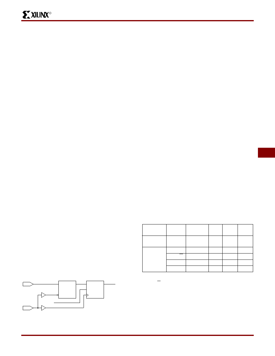
IPAD
BUFGE
BUFGLS
C
CE
DQ
GF
to internal
logic
ILFFX
X9013
Figure 17: Examples Using XC4000X FCL
Table 11: Output Flip-Flop Functionality (active rising
edge is shown)
Mode
Clock
Enable
T
D
Q
Power-Up
or GSR
X
0*
X
SR
Flip-Flop
X0
0*
X
Q
__/
1*
0*
D
XX
1
X
Z
0X
0*
X
Q
Legend:
X
__/
SR
0*
1*
Z
Don’t care
Rising edge
Set or Reset value. Reset is default.
Input is Low or unconnected (default value)
Input is High or unconnected (default value)
3-state
Product Obsolete or Under Obsolescence
相关PDF资料 |
PDF描述 |
|---|---|
| XC4025E-3HQ304C | IC FPGA C-TEMP 5V 3SPD 304-HQFP |
| IDT70V28L20PFI8 | IC SRAM 1MBIT 20NS 100TQFP |
| KMPC8270CVVQLDA | IC MPU PWRQUICC II HIP7 480-TBGA |
| IDT70V28L20PFGI8 | IC SRAM 1MBIT 20NS 100TQFP |
| KMPC8270CVRMIBA | IC MPU PWRQUICC II HIP7 516-PBGA |
相关代理商/技术参数 |
参数描述 |
|---|---|
| XC4025E-4HQ304C | 功能描述:IC FPGA C-TEMP 5V 4 SPD 304-HQFP RoHS:否 类别:集成电路 (IC) >> 嵌入式 - FPGA(现场可编程门阵列) 系列:XC4000E/X 标准包装:1 系列:Kintex-7 LAB/CLB数:25475 逻辑元件/单元数:326080 RAM 位总计:16404480 输入/输出数:350 门数:- 电源电压:0.97 V ~ 1.03 V 安装类型:表面贴装 工作温度:0°C ~ 85°C 封装/外壳:900-BBGA,FCBGA 供应商设备封装:900-FCBGA(31x31) 其它名称:122-1789 |
| XC4025E-4HQ304I | 功能描述:IC FPGA I-TEMP 5V 4 SPD 304-HQFP RoHS:否 类别:集成电路 (IC) >> 嵌入式 - FPGA(现场可编程门阵列) 系列:XC4000E/X 标准包装:1 系列:Kintex-7 LAB/CLB数:25475 逻辑元件/单元数:326080 RAM 位总计:16404480 输入/输出数:350 门数:- 电源电压:0.97 V ~ 1.03 V 安装类型:表面贴装 工作温度:0°C ~ 85°C 封装/外壳:900-BBGA,FCBGA 供应商设备封装:900-FCBGA(31x31) 其它名称:122-1789 |
| XC4025E-4PG223C | 功能描述:IC FPGA C-TEMP 5V 4 SPD 223-CPGA RoHS:否 类别:集成电路 (IC) >> 嵌入式 - FPGA(现场可编程门阵列) 系列:XC4000E/X 标准包装:1 系列:Kintex-7 LAB/CLB数:25475 逻辑元件/单元数:326080 RAM 位总计:16404480 输入/输出数:350 门数:- 电源电压:0.97 V ~ 1.03 V 安装类型:表面贴装 工作温度:0°C ~ 85°C 封装/外壳:900-BBGA,FCBGA 供应商设备封装:900-FCBGA(31x31) 其它名称:122-1789 |
| XC4025E-4PG223I | 功能描述:IC FPGA I-TEMP 5V 4 SPD 223-CPGA RoHS:否 类别:集成电路 (IC) >> 嵌入式 - FPGA(现场可编程门阵列) 系列:XC4000E/X 标准包装:1 系列:Kintex-7 LAB/CLB数:25475 逻辑元件/单元数:326080 RAM 位总计:16404480 输入/输出数:350 门数:- 电源电压:0.97 V ~ 1.03 V 安装类型:表面贴装 工作温度:0°C ~ 85°C 封装/外壳:900-BBGA,FCBGA 供应商设备封装:900-FCBGA(31x31) 其它名称:122-1789 |
| XC4025E-4PG299C | 功能描述:IC FPGA C-TEMP 5V 4 SPD 299-CPGA RoHS:否 类别:集成电路 (IC) >> 嵌入式 - FPGA(现场可编程门阵列) 系列:XC4000E/X 标准包装:1 系列:Kintex-7 LAB/CLB数:25475 逻辑元件/单元数:326080 RAM 位总计:16404480 输入/输出数:350 门数:- 电源电压:0.97 V ~ 1.03 V 安装类型:表面贴装 工作温度:0°C ~ 85°C 封装/外壳:900-BBGA,FCBGA 供应商设备封装:900-FCBGA(31x31) 其它名称:122-1789 |
发布紧急采购,3分钟左右您将得到回复。